Select 5G sinuous waveguide antennas targeting n41/n78 bands (3.3-5GHz), aiming for 15-20dBi gain; ensure ≥800MHz bandwidth and VSWR<1.5 (via HFSS simulation). Choose linear/circular polarization per coverage needs, optimizing impedance for 5G NR efficiency.
Table of Contents
Understanding the Characteristics of Sinusoidal Waveguide Antennas
When selecting antennas for 5G networks, especially in millimeter-wave bands (like 28GHz), the sinusoidal waveguide antenna is an unavoidable high-performance solution. Compared to common microstrip patch antennas, its core advantage lies in its extremely low insertion loss — at 28GHz, its loss can easily be kept below 0.15 dB/m, while the loss of a microstrip line at the same frequency might be as high as 0.5 dB/m or even higher.
For a Massive MIMO antenna integrating 512 antenna elements, using a waveguide structure can increase the system gain by more than 3 dB, equivalent to expanding the effective coverage radius by approximately 20%, or reducing base station power consumption by nearly 30%.
However, the price for this high performance is weight and cost: a 64-port waveguide antenna array may reach a weight of 3-5 kilograms, and its manufacturing cost could be 150% to 200% of a microstrip antenna with equivalent performance. Therefore, understanding its characteristics involves making precise trade-offs between system performance, size/weight, and project budget.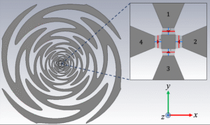
Core Advantages
The free-space path loss of a 28GHz signal is nearly 18 dB higher than at 3.5GHz. This means that to cover the same distance, a millimeter-wave system requires over 60 times the power compensation.
Low Loss: The “Lifeline” of Millimeter-Wave Signals
1. Where Does the Loss Come From: The “Double Taxation” of Conductor and Dielectric
At high frequencies like 28GHz, the skin effect causes current to concentrate only in the conductor’s surface layer, at a depth of about 1.24 micrometers, drastically increasing the equivalent resistance of microstrip lines. Simultaneously, the constant polarization and friction of molecules in the PCB dielectric under the high-frequency alternating electric field generate heat. A typical PTFE-based microstrip line can have a loss of up to 0.4 dB per wavelength at 28GHz. For an array containing a complex power division network, the cumulative loss can easily exceed 3 dB – half the power is lost.
2. The Waveguide Solution: The Energy Highway of Hollow Channels
The inner walls of the waveguide are typically mirror-polished and silver-plated (with surface resistivity as low as ~1.59 μΩ·cm), resulting in conductor loss that can be below 0.08 dB per wavelength at 28GHz. Since the interior is mostly air (dielectric constant ≈1, loss tangent approaching 0), dielectric loss is almost negligible. Replacing the microstrip feed network with a waveguide can directly recover 2-3 dB of “signal wealth” for the system.
3. System-Level Benefits: The Chain Reaction on Coverage, Power Consumption, and Cost
- Coverage Radius Increase: According to wireless propagation models, path loss is proportional to the square (or even a higher power, like 3.5) of the distance. A 3 dB gain can theoretically expand the coverage radius by about 20%. Assuming an originally planned coverage radius of 200 meters, using a waveguide antenna could extend the effective radius to 240 meters.
- Base Station Density and CAPEX Savings: To cover a 1 square kilometer area, the original plan might require about 8 base stations. After a 20% increase in radius, only about 5-6 base stations are needed. Estimating the construction cost per base station (including hardware, site acquisition, construction) at 200,000 RMB, the direct capital expenditure (CAPEX) could be reduced by 400,000 to 600,000 RMB.
- Operational Cost (OPEX) Optimization: Lower loss means the power amplifier (PA) doesn’t need to output higher power for compensation. Assuming a single base station’s power consumption is reduced by 15 watts, and using an industrial electricity price of 0.8 RMB/kWh, a single base station could save about 105 RMB annually in electricity costs. For a network with 10,000 base stations, annual electricity savings could exceed 1 million RMB. Additionally, reduced heat generation allows for simpler cooling system design, further lowering failure rates and maintenance costs.
High Power Capacity: The “Sturdy Chassis” Supporting Complex Signals
1. Physical Basis of Power Capacity: The Breakdown Field Strength of the Air Dielectric
At standard atmospheric pressure, air’s breakdown field strength is about 3 kV/mm. A standard WR-28 waveguide (internal dimensions 7.112mm x 3.556mm) operating at 28GHz can theoretically have a peak power capacity exceeding 2 kilowatts.
In contrast, the power capacity of a microstrip line is limited by the width of its thin conductor strip (possibly only 0.5mm) and the thermal conductivity of the substrate material (e.g., thermal conductivity of 0.2-0.3 W/(m·K)), typically restricting its average power capacity to 50-100 watts.
2. Addressing the Peak-to-Average Power Ratio (PAPR) Challenge of 5G Signals
5G signals use multi-carrier technologies like OFDMA, resulting in a Peak-to-Average Power Ratio (PAPR) that can be as high as 10-12 dB. This means that for a power amplifier with an average output power of 10 watts, the instantaneous peak power might reach 100 watts or more.
Microstrip line systems operating near such high peak powers can easily enter the non-linear region, generating intermodulation distortion (IMD) and degrading signal quality. The massive power headroom of waveguide antennas (>1 kW) ensures linear signal transmission even under the most complex modulations (like 1024QAM), which is fundamental for achieving Gbps data rates.
3. Synergy with Massive MIMO and Beamforming
Massive MIMO systems work by coordinating 64 or even 256 antenna elements to form high-gain pencil beams. While the power per channel is low (e.g., ~250mW), the power superposition at the beamforming focal point from all channels is significant.
The waveguide structure can not only withstand this concentrated power but its inherent high port-to-port isolation (typically >30 dB) also effectively prevents energy coupling between channels, ensuring the precision of beamforming and suppressing sidelobe levels below -15 dB, thereby reducing inter-cell interference.
Inherent Disadvantages
In the 28GHz band, a 64-port waveguide antenna array can easily weigh over 3.5 kilograms, with a volume of about 300mm x 300mm x 50mm, and an estimated unit manufacturing cost of $800 to $1200.
In comparison, a microstrip patch antenna of equivalent specifications might weigh less than 1.2 kilograms, have a volume 30% smaller, and cost less than $300. This more than double the weight, larger volume, and over three times the cost are facts that every network architect must confront at the design stage.
These disadvantages cannot be eliminated through simple optimization; they directly impact deployment difficulty, tower load-bearing, wind load design, and the project’s Return on Investment (ROI).
Physical Size
1. The Size Redline Set by the Cut-off Frequency
For the most common rectangular waveguide, the relationship between the cut-off wavelength λc of the dominant mode (TE10 mode) and the broad wall dimension ‘a’ is λc = 2a. This means the broad wall ‘a’ must be greater than half the operating wavelength.
- Data Example: For a 28GHz signal, its wavelength in air is approximately 10.7 millimeters. Therefore, the broad wall ‘a’ of the waveguide carrying it must be greater than 5.35 millimeters. This is the theoretical minimum; in practical designs, to ensure performance and accommodate tolerances, a larger size is typically chosen, such as the standard WR-28 waveguide’s ‘a’ dimension of 7.11 mm.
- Comparison with Microstrip: The radiating element size of a microstrip patch antenna is approximately equal to half the wavelength in the dielectric, but its feed network is etched onto a very thin circuit board. A 28GHz microstrip patch might have a width of only 3-4 mm, and the entire array can share an extremely thin dielectric substrate, with an overall thickness potentially below 1 mm. In contrast, a waveguide is a three-dimensional structure, and its height (the ‘b’ dimension) also has requirements (the ‘b’ dimension of WR-28 is 3.56 mm). This makes the longitudinal dimension of a multi-layer waveguide array much larger than that of a microstrip circuit.
2. The Natural Bottleneck in Array Integration Density
A waveguide antenna array is fabricated by precisely machining and assembling a large number of independent, hollow metal cavities. Each unit is like a “small room.”
The element spacing can be compressed to about 0.7 wavelengths, whereas the element spacing in a waveguide array is limited by mechanical wall thickness, typically around 0.8-0.9 wavelengths, which somewhat limits the efficiency of the antenna aperture utilization.
Weight
1. The Weight of the Material Itself
Waveguide antennas are typically made from aluminum alloy (density ~2.7 g/cm³) or copper alloy (density 8.9 g/cm³) via precision CNC machining or die-casting. A 28GHz waveguide array with 256 radiating elements might have a total metal volume of about 800 cm³, with the material weight alone exceeding 2.1 kilograms. This doesn’t include the weight of mounting brackets, sealing materials, and the protective radome.
2. The “Weight Tax” in Deployment
The increase in antenna weight is not an isolated issue; it triggers a chain reaction of costs and engineering challenges:
- Tower and Bracket Reinforcement: A 5 kg antenna on a tower tens of meters high, subjected to wind speeds of 40 m/s (Category 12 typhoon), generates an overturning moment that requires stronger support structures to counteract, increasing the cost of these steel structures linearly.
- Installation and Maintenance: Increased weight means requiring more specialized lifting equipment (e.g., large hydraulic lifts) and more installation personnel. Assuming installing a microstrip antenna requires 2 workers taking 1 hour, installing a waveguide antenna might require 3 workers and take 1.5 hours. Labor costs and equipment rental fees increase accordingly. Subsequent maintenance, like antenna replacement, becomes more difficult and risky.
- Wind Load and Safety: Larger frontal area and weight mean greater wind load. This necessitates stricter safety checks for the tower structure. In some high-wind-disaster areas, desired site locations might even be unattainable due to antenna weight and wind load exceeding standards.
Manufacturing Cost
1. The Trade-off Between Machining Precision and Yield
To ensure excellent electrical performance (e.g., return loss < -15 dB across the operating band), the dimensional tolerances for the waveguide’s internal features must be controlled within extremely strict limits. For millimeter-wave bands, this tolerance is typically required to be within ±0.02 mm to ±0.05 mm. This relies on high-precision five-axis CNC machines (equipment cost can reach hundreds of thousands to millions of dollars) or high-mold-cost precision die-casting processes.
During machining, any minor tool wear or temperature fluctuation can cause dimensions to fall outside tolerance, resulting in scrap. The yield for a complex waveguide array might initially be only 70%-80%, meaning 20%-30% of the cost is分摊 by scrap parts.
2. Complexity of Process Steps and Cost Stacking
Manufacturing a complete waveguide antenna array involves far more than just “cutting”:
- Multi-Part Assembly: An array might consist of dozens or even hundreds of independent waveguide cavities that need to be combined via welding (like vacuum brazing) or screw fastening. Welding requires specialized jigs and furnaces and can cause thermal distortion; screw fastening requires designing complex flanges and sealing structures, consuming significant labor for assembly and alignment.
- Surface Treatment: To further reduce conductor loss, the inner walls of the waveguide are often silver-plated (silver has higher conductivity than aluminum or copper). This adds the cost of the plating process and environmental treatment fees.
- Seal Testing: Being a hollow structure, airtightness must be guaranteed to prevent moisture ingress affecting performance. This requires 100% helium mass spectrometry leak testing or similar seal tests, representing an additional quality cost.
3. Cost Structure Comparison with PCB Antennas
Microstrip antennas use standard Printed Circuit Board (PCB) processes. Using ultraviolet photolithography and etching, hundreds or even thousands of antenna arrays can be produced simultaneously on a large panel exceeding 1 square meter in area.
When production volume reaches the level of 100,000 units, the cost per antenna is primarily determined by the price of the copper-clad laminate material (like Rogers RO3003), and the processing cost is diluted to a very low level.
In contrast, waveguide antenna manufacturing is essentially “subtractive machining” and “precision assembly,” resulting in low material utilization and limited automation. This causes its cost curve to decrease with volume much slower than that of PCB antennas. Even at volumes of hundreds of thousands, it’s difficult for waveguide antenna costs to fall below 1.5 times that of PCB antennas.
Core Application Scenarios
In the overall investment of a 5G network exceeding millions, the difference in antenna selection might only account for a fluctuation of tens of thousands, but the chain reaction it triggers can affect the entire project’s payback period. The cost of a sinusoidal waveguide antenna, up to 3 times that of a ordinary antenna, forces decisions to be precise for each specific scenario.
In millimeter-wave bands, its low-loss characteristic might extend the base station coverage radius from 200 meters to 240 meters, equivalent to reducing the number of base stations needed to cover 1 square kilometer by 2, directly saving over 400,000 RMB in hardware and site costs. Conversely, in indoor Sub-6GHz environments where signal attenuation is inherently lower, the same investment might yield negligible performance gains. The criterion is: Are the signal path loss and system power budget so severe that a waveguide antenna is necessary to “salvage” every decibel of gain?
Scenarios Where This Cost is Non-Negotiable
1. Millimeter-Wave Macro Base Stations and Fixed Wireless Access in Urban Hotspots
In urban core areas with population densities exceeding 15,000 people per square kilometer, the demand on 5G networks is to provide user experience rates above 1 Gbps. Millimeter waves at 28GHz or 39GHz are the only bands offering contiguous bandwidths of 800 MHz or more.
- Performance Bottleneck: Millimeter-wave signals have very poor penetration; even a leaf or rain can cause significant attenuation. Non-Line-of-Sight (NLOS) transmission in dense urban areas relies on complex reflections and diffraction. The signal reaching the user might have attenuated by 110-130 dB. In such cases, the Equivalent Isotropically Radiated Power (EIRP) of the antenna system is crucial.
- Value of Waveguide: A 64-port millimeter-wave Massive MIMO base station might have a transmit power around 40 dBm. If using a microstrip antenna, the feed network loss could be as high as 3 dB, meaning half the power is wasted. Switching to a waveguide antenna can control this loss to within 1 dB, equivalent to gaining 2 dB of free transmit power for the base station. This 2 dB directly translates to the user’s mobile phone receiving a signal strength of -93 dBm instead of -95 dBm at a building corner or near a window, significantly improving connection stability. The drop-out rate might decrease from 5% to below 1%. This investment directly purchases network reliability and user satisfaction.
2. High-Capacity Millimeter-Wave Backhaul Links for Network Backbone
In areas where fiber is difficult to reach or deployment costs are prohibitive, millimeter-wave point-to-point backhaul is a mainstream solution, requiring link availability of 99.999%.
- Stringent Requirements: An 80GHz (E-Band) backhaul link with a transmission distance of 1 kilometer already has a free-space path loss exceeding 130 dB. To guarantee a 2 Gbps transmission rate and withstand rain fade (additional loss under moderate rain can be 20 dB/km), antennas at both ends need very high gain (typically >45 dBi).
- Necessity of Waveguide: Achieving such high gain requires a large antenna aperture (typically diameter 60-90 cm). If a microstrip feed network were used for such a large aperture, the cumulative loss would be considerable. The low-loss advantage of waveguide antennas is magnified immensely at such high frequencies and gain requirements. At 80GHz, reflector or lens antennas with waveguide feeds can achieve efficiencies over 70%, while other solutions might be below 50%. This ensures the link maintains the minimum required Signal-to-Noise Ratio even in extreme weather, avoiding outages.
Scenarios Where Cost-Saving is Advisable
1. Wide-Coverage Macro Base Stations in Sub-6GHz Bands
The signal wavelength in the 3.5GHz band is about 8.6 cm, with path loss far lower than millimeter waves. Coverage is the primary goal, with a base station typically needing to cover a radius of 500-1000 meters.
- Performance Overkill: At this distance, path loss is the main challenge. The antenna’s own feed loss (even the 1-1.5 dB of a microstrip line) has relatively minor impact. Using a waveguide antenna might reduce loss by another 0.5 dB, but the improvement in coverage range is minimal, perhaps only 10-20 meters.
- Economic Consideration: A 3.5GHz Massive MIMO antenna using microstrip technology might cost around 4,000 RMB, while a waveguide solution could exceed 10,000 RMB. Paying a 150% premium for negligible coverage improvement is uneconomical. The saved funds could be used to deploy an additional base station, resulting in better overall network coverage.
2. Indoor Small Cells and Enterprise-Level Picocells
Indoor scenarios are characterized by short coverage distances (<50 meters), fluctuating user capacity demands, and requirements for compact antenna size and aesthetics.
- Loss is Not a Critical Factor: Over short distances of tens of meters, the signal strength is inherently strong. A difference of 1 dB or 0.5 dB in antenna loss is barely perceptible to the user experience. For devices deployed on ceilings or walls, weight and volume are more critical considerations. A 1 kg microstrip antenna is easy to install, while a 3 kg waveguide antenna might require additional reinforcement, increasing deployment complexity and cost.
- Intense Cost Pressure: Enterprise network procurement is highly price-sensitive. The total equipment cost for an indoor small cell supporting 200 concurrent users in an office might be around 50,000 RMB. If using a waveguide antenna causes a price increase of 20% (10,000 RMB), it could potentially cause the project to be abandoned. In this scenario, microstrip antennas offer the best cost-performance ratio.
Considering Antenna Structure and Integration
The internal structural design of the antenna and how it integrates with your system directly determine the performance ceiling, reliability, and total cost.
Especially at millimeter-wave frequencies like 28GHz or 39GHz, every 0.5dB increase in transmission line loss can shrink the system’s coverage radius by over 10%.
A superior design can expand your base station’s coverage by 30%, while a poor integration scheme might result in overall performance not even reaching 70% of the theoretical value.
Array Scale
In the millimeter-wave band, the radiation capability of a single antenna element is extremely limited. At 28 GHz, a standard sinusoidal waveguide element has a gain of only about 6 dBi, with a half-power beamwidth potentially wider than 80 degrees – like a dim light bulb, energy is dispersed and travel distance is short, utterly failing to meet the hundreds of meters coverage requirement of 5G base stations. Combining tens or even hundreds of elements into an array is the only engineering method to boost gain above 25 dBi and narrow the beam to within 5 degrees.
Number of Elements vs. Gain is a Logarithmic Relationship
The gain increase follows the formula 10log10(N). This means gain scales logarithmically, not linearly, with the number of elements. Increasing from 1 to 4 elements (a 2×2 array), N=4, 10log10(4) ≈ 6 dB, total gain = 6 dBi + 6 dB = 12 dBi.
But increasing from 4 to 16 elements (4×4 array), N=16, 10log10(16) = 12 dB, you added 12 elements but gain only increased by 12 dB - 6 dB = 6 dB compared to the 4-element array. Increasing from 16 to 64 elements (8×8 array), N=64, 10log10(64) = 18 dB, you added 48 elements, but gain only increased by 18 dB - 12 dB = 6 dB. Returns are diminishing: Quadrupling the number of elements only doubles the gain (adds 6 dB). Going from 64 to 256 elements (16×16) requires adding 192 more elements for just another 24 dB - 18 dB = 6 dB gain.
Array Aperture Size Directly Determines Beamwidth
Beamwidth (θ) is primarily determined by the array’s physical size (D) and the operating wavelength (λ), approximated by θ ≈ k * λ/D (k is a constant, typically between 50 and 70). For a given frequency band (fixed λ), beamwidth is inversely proportional to array size.
An 8×8 array operating at 28 GHz (wavelength λ≈10.7mm), with an element spacing of 0.7λ (approx. 7.5mm), has an aperture size of about 8 * 7.5mm = 60mm. Its horizontal beamwidth is approximately 65 * (10.7 / 60) ≈ 11.6 degrees.
Scaling the array to 16×16, aperture size becomes 16 * 7.5mm = 120mm, and beamwidth narrows to about 65 * (10.7 / 120) ≈ 5.8 degrees. This narrow 6-degree beam acts like a precise laser pointer, enabling long-distance point-to-point transmission but requiring high alignment stability between base station and user equipment – slight jitter can cause link failure. Conversely, a 4×4 array has a beamwidth of about 23 degrees, offering wider coverage, more suitable for small cells needing to cover a sector.
Element Spacing is a Hidden “Trap”
Element spacing (d) cannot be set arbitrarily. To avoid undesirable grating lobes (energy radiating from multiple directions), d must satisfy d < λ / (1 + |sinθ|), where θ is the maximum scan angle.
For a phased array requiring ±60 degree scanning, d typically must be less than 0.65λ. If d is set too large, say 0.9λ, when the beam scans to 30 degrees, a grating lobe comparable in strength to the main lobe might appear, wasting energy and causing interference.
But d cannot be too small either; less than 0.5λ increases mutual coupling between elements, reducing antenna efficiency. Therefore, d is usually strictly confined to the narrow window between 0.5λ and 0.7λ.
Rectangular Array vs. Linear Array: A Shape Game
We often discuss square arrays (M x M), but rectangular arrays (M x N, M≠N) are more common in practice. A 16 x 4 (64 elements) rectangular array has different beamwidths in the horizontal and vertical planes. The horizontal direction has 16 elements, resulting in a narrow beam; the vertical direction has only 4 elements, resulting in a wider beam. This array produces a horizontally narrow, vertically wide “fan” beam, ideal for deployment on rooftops needing to cover the street below. An 8 x 8 (also 64 elements) square array produces a symmetric “pencil” beam, suitable for point-to-point communication.
The Scaling Ceiling is Limited by Cost and Integration
A 256-element array requires 256 independent feed points. If it’s an active phased array, this corresponds to 256 sets of phase shifters, attenuators, and amplifier channels. The challenges are:
- Cost: RF chip cost is almost proportional to the number of channels. A 256-channel solution might cost 3-4 times more than a 64-channel solution, not increasing linearly.
- Power Consumption and Heat Dissipation: 256 RF front-ends operating simultaneously can consume 20-30 watts, generating heat that requires complex thermal management. If the chip junction temperature exceeds 125°C, performance degrades or damage occurs.
- Calibration Complexity: Calibrating the amplitude and phase of 256 channels requires significantly more time and data than a 64-channel array, increasing production test cost and time.
Therefore, in 5G millimeter-wave base stations, 64-element and 256-element are two mainstream configurations, striking different balances between performance, cost, and size. The choice depends on your link budget, equipment pricing, and the hard constraints of the installation environment.
Feed Network
At 28 GHz frequency, the conductor and dielectric losses of ordinary PCB microstrip lines can easily reach 0.7 dB/cm. This means that in a 64-element array measuring 6 cm x 6 cm, the signal path from the input port to the farthest radiating element might exceed 10 cm, resulting in a one-way loss as high as 7 dB. This is equivalent to over 80% of the power from your power amplifier’s 500 milliwatt output being converted to heat inside the antenna itself before reaching the edge elements; only about 100 milliwatts arrives.
How You “Feed” the Signal to Each Element
- Corporate Feed (Parallel/Side Feed): Like a river’s main channel splitting into multiple branches simultaneously. Uses T-junctions or Wilkinson power dividers to distribute power stage by stage. Its biggest advantage is that all path lengths are equal; signals arrive at each element simultaneously, providing true time delay. This allows the antenna to operate over a very wide bandwidth (e.g., 24-30 GHz, relative bandwidth over 20%) with almost no beam squint (beam squint effect less than 2 degrees). Disadvantages include complex structure, large area occupation, increased routing, and loss. The insertion loss of a single-stage power divider is typically 0.2-0.3 dB. After 6 stages (2^6=64) of division, the cumulative loss from the dividers alone might reach 1.5 dB or more.
- Series Feed (End Feed): Like a string of beads, the signal couples from one element to the next. Structure is compact, with almost no area waste. But a fatal flaw is the unequal path lengths, causing significant beam pointing shift with frequency. At 28 GHz the beam points at 0 degrees, but at 26 GHz it might shift to -10 degrees, and at 30 GHz to +8 degrees. This limits its use to very narrow bandwidth applications (< 2%). The tolerance requirements for inter-element coupling are extremely high; a ±5% deviation can cause amplitude distribution imbalance, raising sidelobe levels by 3-5 dB.
- Hybrid Feed: Combines the advantages of both. For example, using a 4-way corporate feed in the horizontal plane for bandwidth, with each branch connecting to a 16-element series feed network to save space. This design requires careful trade-offs between bandwidth, complexity, and performance.
Line Loss
- Microstrip Line: Simple fabrication, low cost, but energy is partly in air, partly in dielectric, resulting in higher loss. At 30 GHz, using a 0.508 mm thick Rogers 5880 substrate, microstrip loss is about 0.25 dB/cm. Using cheaper, higher-loss materials like FR-4, loss can soar above 0.5 dB/cm.
- Stripline: The signal line is embedded between two dielectric layers, reducing radiation loss, but fabrication is more complex, requiring good lamination工艺. Loss is slightly lower than microstrip, about 0.2 dB/cm.
- Substrate Integrated Waveguide (SIW): A row of metallized vias in the dielectric substrate forms a waveguide-like enclosed structure. This is a mainstream technology for low-loss (can be below 0.1 dB/cm) feed networks at millimeter waves. However, the width of SIW is frequency-dependent; at 28 GHz, the width is about 4 mm, which can limit the reduction of element spacing, potentially causing grating lobes. The via diameter and spacing must be fractions of a wavelength, typically requiring diameter >0.2 mm and spacing <1 mm, posing a severe test for PCB fabrication precision.
Substrate Material Determines the Loss Floor
The substrate material’s Dielectric Constant (Dk) and Loss Tangent (Df) are decisive parameters.
- Standard FR-4: Dk≈4.3, Df≈0.02@10GHz. Low cost, but Df increases significantly with frequency, loss is very high at 28 GHz, and dielectric constant uniformity can vary over 5%, causing phase inconsistency. Generally unsuitable for millimeter-wave arrays.
- PTFE-based materials (e.g., Rogers 5880): Dk≈2.2, Df≈0.0009. The preferred choice for high-performance antennas, with extremely low loss. But cost is 20-30 times that of FR-4, mechanical strength is slightly poorer, and the coefficient of thermal expansion is high.
- Hydrocarbon/Ceramic-filled (e.g., Rogers 4350B): Dk≈3.48, Df≈0.0031. A balance between performance, mechanical strength, and price. A compromise choice for many base station antennas. Loss is higher than PTFE but acceptable and cost-controllable.
Choosing high-precision laminates with Dk tolerance controlled within ±0.05 ensures phase consistency error less than 2 degrees.
Uneven Power Distribution
- Amplitude Error: Due to manufacturing tolerances, the power reaching each element might vary by ±0.5 dB. This raises the sidelobe level of the antenna pattern. Controlling the standard deviation of amplitude error within 0.3 dB is a basic requirement for keeping sidelobes below -20 dB.
- Phase Error: This is more critical. Path length differences and material non-uniformity introduce phase errors. A root mean square (RMS) phase error of 10 degrees reduces antenna gain by about 0.3 dB, and a 15 degree error raises sidelobes by 2-3 dB. Post-fabrication, phase compensation via laser trimming or programmable phase shifters is often necessary.
Beamforming Integration
In the 5G millimeter-wave band, propagation loss is huge, and signals are easily blocked. A fixed narrow beam cannot track moving users, causing frequent link failures. Beamforming integration is the core technology that upgrades this “fixed flashlight” into an “intelligent spotlight.”
It involves integrating an independent RF transceiver channel (typically including Power Amplifier PA, Low-Noise Amplifier LNA, Phase Shifter, and Attenuator) behind each antenna element. Using algorithms to control the phase of the RF signal in each channel in real-time enables inertialess, microsecond-level electronic beam scanning.
A typical 256-element millimeter-wave active phased array may contain over a billion transistors internally, representing the pinnacle of millimeter-wave front-end technology.
Chips are the Brain
- Phase Shifter: Precisely Controls Beam Direction: The number of bits in the phase shifter determines the minimum phase step. A 1-bit phase shifter has only 0° and 180° states, insufficient accuracy. A 5-bit phase shifter provides 32 (2^5) phase states, with a minimum step of 11.25°, common in early designs. The current mainstream is 6-bit precision, providing 64 states, minimum step 5.625°, keeping beam pointing error within 1°. High-end designs use 7-bit or even 8-bit phase shifters for steps of 2.8° or less, meeting the demands of multi-user MU-MIMO scenarios. Phase shifter insertion loss is typically 6-10 dB, which must be compensated for in the system gain budget.
- Attenuator: Shapes the Beam and Aids Calibration: Similar to phase shifters, attenuators are typically 5-bit or 6-bit, providing 1 dB or 0.5 dB steps, with a dynamic range of about 20-30 dB. Its core roles are: 1) Applying tapering (amplitude weighting) during beam scanning to suppress sidelobes (e.g., -25 dB sidelobes might require 8-10 dB attenuation for edge channels); 2) Calibrating the ±1.5 dB amplitude inconsistency among channels due to manufacturing tolerances.
- Amplifiers and Noise: The Cornerstone of the System Link: The output power of each channel’s Power Amplifier (PA) is limited at millimeter waves. At 28 GHz, the single-channel output power at the 1 dB compression point (P1dB) is typically on the order of 10-15 dBm (10-30 milliwatts). After spatial combining of 256 channels, the total Equivalent Isotropically Radiated Power (EIRP) can reach 40-50 dBm (10-100 watts). The Noise Figure (NF) of the Low-Noise Amplifier (LNA) is critical. Reducing the noise figure by 1 dB increases receiver sensitivity, potentially expanding coverage by 10-15%. Advanced LNA noise figures using SiGe or CMOS technology can be 3.5-4.5 dB.
Material and Process Choice: A Performance vs. Cost Game
- Low-Temperature Co-fired Ceramic (LTCC): Due to its multi-layer wiring capability, excellent thermal conductivity (thermal conductivity ~2-3 W/m·K), and ability to embed passive components, it was common in early and high-reliability applications. But its dielectric constant is usually high (5.0-7.0), leading to larger circuit sizes, and processing cost is high. Line width/spacing precision is typically around 50 microns.
- High-Performance Laminates (e.g., Panasonic Megtron 6, Rogers series):They offer lower dielectric constant (3.0-3.5) and loss, support finer lines (width/spacing can reach 25μm/25μm), and cost less than LTCC. Using Any-layer HDI processes enables high-density interconnects, facilitating integration of large arrays. But their Coefficient of Thermal Expansion (CTE) must match the chips, otherwise solder joint fatigue failure can occur during temperature cycling (-40°C to +85°C).
- Semiconductor Processes (Si, GaAs): Beamforming chips fabricated using 45 nm CMOS RF-SOI or 0.15 μm GaAs pHEMT processes are the core for high integration. CMOS offers low cost, high integration (digital control and RF front-end on the same chip), but output power and linearity are slightly inferior. GaAs offers higher output power and better linearity, but cost and integration are lower than CMOS.
Calibration is an Unavoidable Hurdle in Mass Production, Directly Determining Yield
Due to the extremely short millimeter wavelength (~10.7 mm at 28 GHz), micron-level manufacturing tolerances introduce significant phase errors. A 256-channel array must undergo full channel amplitude and phase calibration before leaving the factory.
- Near-Field Calibration: In an anechoic chamber, a probe measures the radiated field of each channel at a distance of 3-5 wavelengths (approx. 30-50 cm) from the antenna aperture. Iterative algorithms calculate the required compensation values for each channel (phase compensation range might be ±40°, amplitude compensation ±3 dB), which are written to the chip’s non-volatile memory. This process takes 5-10 minutes per antenna, a significant part of production cost.
- Built-In Self-Test (BIST): To reduce cost, some advanced chips integrate BIST functionality. Using internal coupling and detection circuits, some parameters can be self-tested and calibrated without radiating, potentially reducing production line calibration time to under 1 minute, but this greatly increases chip design complexity.
Thermal Management is the Lifeline of Reliability
A 256-channel active array, even at medium power, can have a total power dissipation of 15-25 watts. This heat is concentrated on a substrate area possibly smaller than 50 cm², resulting in a power density of 0.3-0.5 W/cm².
- Heat Conduction Path: Heat must travel from the chip junction, through solder bumps, the substrate, and finally to a metal heat sink. The thermal resistance of each step must be carefully designed. The junction-to-case thermal resistance (θ_JC) might be 5-10 °C/W. Using Thermal Interface Material (TIM) between the case and heat sink adds resistance of maybe 1-2 °C/W.
- Junction Temperature Control: Assuming total power 20W, total thermal resistance 5 °C/W, at an ambient temperature of 55°C, the chip junction temperature would be 55 + (20 * 5) = 155°C. This is near or exceeds the maximum junction temperature for many semiconductors (150°C). Therefore, high thermal conductivity metal heat sinks (e.g., aluminum alloy, ~200 W/m·K) or even embedded heat pipes (effective thermal conductivity up to thousands of W/m·K) with forced air cooling are essential to keep the junction temperature below 125°C, ensuring a lifespan exceeding 5 years. Failure analysis shows that for every 10°C increase in junction temperature, device lifetime halves.
Selecting the Antenna Structure
For a 28GHz small cell antenna, if the cost must be controlled within 15% of the total BOM cost and it must operate stably from -40°C to +85°C, then SIW might be the only feasible option.
Conversely, for an E-Band (80GHz) point-to-point long-distance backhaul link, where the primary goals are transmission loss below 0.1 dB/km and 99.999% reliability, even if metal waveguide costs 3-5 times more, it is the unequivocal choice.
Core Showdown
For a micro cell antenna design target of 28GHz, 200MHz bandwidth, 15dBi gain, using an SIW solution might keep the BOM cost under 80 RMB, weight less than 150 grams, but the total link insertion loss might reach 2.5 dB. Achieving the same electrical specifications with an aluminum die-cast waveguide would immediately drive the cost to over 300 RMB, weight over 800 grams, but would deliver an extremely low loss of 1.2 dB. This 1.3 dB difference and 220 RMB price difference is the core trade-off you need to evaluate using system-level metrics.
Just How Expensive Is This Thing?
For a 16-element linear array operating at 28GHz, you’d need high-frequency laminates like Rogers RO4350B (Dk 3.66±0.05, Df 0.0031@10GHz), costing about 0.8 RMB per square centimeter. Adding standard PCB processes like laser drilling, plating, patterning, and etching, the core component cost can be controlled within 30-50 RMB.
First, you need a die-cast blank of ADC12 aluminum alloy or a forged blank of oxygen-free copper. Machining a waveguide cavity requiring an internal surface finish of Ra < 0.8μm requires high-speed CNC machines for hours of milling and drilling. For a 200 mm long waveguide antenna, just the machining cost could exceed 150 RMB. This doesn’t include the labor cost for manual tuning to ensure port return loss better than -55 dB, nor the final silver plating (2-3μm thick) surface treatment cost. Overall, the direct cost of a metal waveguide antenna is easily 3 to 8 times that of SIW.
How to Fit It Into a Compact Device?
Integration level determines product design freedom. SIW’s inherent advantage is planar form factor. You can integrate the antenna, feed network, and even filters and phase shifters on the same 0.508 mm thick circuit board. The entire RF front-end can be mounted like a stamp inside the device housing, with total thickness under 3 mm. This is the only option for mobile phones or Customer Premises Equipment (CPE) with extremely strict thickness tolerances.
Metal waveguide is a three-dimensional structure. A standard WR-28 waveguide (for 26.5-40GHz) has internal cross-section 7.112 x 3.556 mm, but ensuring structural strength and wall thickness, the external dimensions typically reach 10 x 6 mm. Making a 4×4 planar array, the entire antenna module thickness (including mounting flange) is hard to keep below 15 mm. More critically is the connection; you need a precise waveguide-to-microstrip transition, which itself introduces an additional loss of 0.3 to 0.5 dB and increases assembly complexity and tolerance sensitivity.
How Far Can the Signal Go, How Much Energy is Lost?
This is the core of the performance showdown, directly related to link budget and coverage. Signal attenuation comes mainly from conductor and dielectric losses.
In the 39GHz band, a 10 cm long SIW transmission line, combining conductor loss (due to the metal via array walls not being ideal conductors) and dielectric loss (from the PCB material), might have a total insertion loss varying between 1.8 dB to 3 dB, highly dependent on the substrate’s loss tangent. For example, Rogers RO3003 has tanδ=0.0010, while Taconic TLY-5 has tanδ=0.0009 – this small difference accumulates into noticeable performance variation at mmWave.
For a standard rectangular waveguide (WR-22) of the same length and frequency band, since the wave propagates in pure air dielectric confined by highly conductive metal walls, its insertion loss can easily be below 0.5 dB.
In long-distance backhaul systems requiring gains above 30 dBi, this over 2 dB loss difference could shorten the transmission distance by over 20%, or require increasing transmit power by 60% to compensate, putting significant pressure on PA cost and device power consumption.
Can It Withstand High Power and Harsh Weather?
Reliability is the cornerstone of device lifespan, especially outdoors. SIW’s power handling is limited by the substrate’s thermal decomposition temperature and the conductor’s current density. Common PTFE-based laminates (like RO4350B) typically handle continuous power in the tens of watts range. Under mismatch conditions like VSWR > 3:1, reflected energy quickly turns to heat, potentially causing delamination or copper peel-off.
Metal waveguide is inherently a high-Q resonant cavity, made from a solid metal block with excellent conductivity. A copper WR-90 waveguide (X-band) can handle kilowatts of average power. For the common 40W average power scenario in 5G base stations, metal waveguide has ample margin and极高 reliability.
The metal waveguide cavity itself is airtight. Just ensuring seal at the flange interfaces naturally achieves IP67 protection rating. It easily withstands temperature cycling from -55°C to +125°C with minimal performance variation.
For SIW antennas, the PCB material (e.g., FR-4 substrate) and copper foil have different Coefficients of Thermal Expansion (CTE). After experiencing 1000 cycles from -40°C to +85°C, vias and plating may develop fatigue cracks, causing gradual performance degradation.
In 95% humidity, if the conformal coating is defective, moisture ingress can significantly alter the substrate’s effective dielectric constant, causing a center frequency shift over 100 MHz.
Decision Matrix
For requirements at 28GHz of 18 dBi gain and operating temperature -40°C to +85°C, with a unit procurement budget strictly capped below 120 RMB – in this case, the metal waveguide quote might not even pass; you must prioritize solving SIW’s heat dissipation and protection issues.
Conversely, if the specification requires E-band (80GHz) backhaul link availability of 99.999% and cumulative downtime not exceeding 105 minutes over a 20-year lifespan, then even if SIW saves 70% cost, its potential reliability risks rule it out.
Step 1: Budget and Volume
- When your project is in the prototype or low-volume phase (< 1000 units):
- Situation Analysis: The cost for a precision mold for metal waveguide (e.g., die-casting mold) can be 150,000 to 300,000 RMB. This high Non-Recurring Engineering (NRE) cost. E.g., a 200,000 RMB mold cost for 500 units adds 400 RMB per unit just for mold amortization.
- Decision Path: In this case, prioritize the SIW solution, even using more expensive but readily sample-able RF laminates (like Rogers RO5880). Leveraging the PCB industry’s quick-turn prototype services, you can get functional samples within 1 week for a cost of a few thousand RMB, significantly reducing upfront investment and trial-and-error cost. The SIW solution typically has absolute cost and speed advantages for volumes below 1000 units.
- When your project enters mass production (> 100,000 units):
- Situation Analysis: The situation may reverse. SIW cost is primarily the high-frequency laminate, a variable cost – higher volume means higher total material cost. For metal waveguide, after the mold cost is amortized, the unit material cost (aluminum ingot or copper) becomes very low. For a complex waveguide array in mass production, the aluminum cost might be only 20-30 RMB.
- Decision Path: You need precise quotes from suppliers based on 100,000 units/year volume. If the metal waveguide quote can drop to within 1.5 times the SIW solution (e.g., SIW at 50 RMB, metal waveguide at 75 RMB), and it offers a performance advantage of >0.5 dB, then the metal waveguide, due to its higher reliability, might be the better long-term choice. Mass production volume amplifies the cost competitiveness of metal waveguides.
Step 2: Define Your Performance Baseline
- Scenario A: The signal needs to travel a long distance (>1 km) or penetrate multiple walls.
- Quantitative Analysis: Assume your system link budget is very tight, with less than 1 dB margin for total insertion loss. This means the antenna’s own efficiency is critical.
- Decision Path: Almost certainly must choose metal waveguide. For example, in a 60GHz backhaul link, the loss from the feed point to the radiating aperture for SIW might be 3.5 dB, while metal waveguide can achieve below 1.0 dB. This 2.5 dB difference in the free-space path loss formula corresponds to roughly a 30% reduction in transmission distance. In a link-budget-tight system, every decibel is invaluable.
- Scenario B: Signal coverage is within 200 meters, and Line-of-Sight conditions are good.
- Quantitative Analysis: The link budget is ample here, likely with 10 dB or more margin. Sacrificing 1-2 dB of antenna efficiency for significant cost reduction is wise.
- Decision Path: The SIW solution becomes the preferred choice. You can accept its 2.0 dB insertion loss and invest the saved cost into other parts of the RF front-end, such as a better-performing Low-Noise Amplifier (LNA) with filtering, whose improvement in system noise figure might be far more important than the antenna’s loss.
Step 3: Evaluate Your Installation and Operational Environment
- Environmental Stress 1: Severe Temperature Cycling.
- Specific Challenge: In deserts or highlands with daily temperature variations exceeding 50°C, the threat to SIW antennas is CTE mismatch between different materials. The PCB dielectric, copper foil, and soldered components have different CTEs. Over a 10-year lifespan with tens of thousands of thermal cycles, vias and solder joints can fracture due to fatigue.
- Decision Path: If the operating temperature range requirement exceeds -40°C to +105°C, or the number of daily temperature cycles exceeds 2, prioritize evaluating metal waveguide. The monolithic nature and thermal stability of metal structures far surpass composite materials.
- Environmental Stress 2: High Humidity, Salt Fog, and Chemical Corrosion.
- Specific Challenge: In coastal or industrial areas, airborne chloride ions (salt fog) and sulfides are killers. While metal waveguides are robust, if surface treatment is inadequate (e.g., plating thickness <5μm or presence of pinholes), corrosion can occur within 18 months, leading to sharply increased loss. SIW antennas fear moisture ingress into the substrate, changing the dielectric constant and causing a center frequency shift up to 2%.
- Decision Path: This isn’t a simple either/or. You need to compare specific processes: An aluminum alloy waveguide with thick gold plating or passivation over 10μm typically has better corrosion resistance than an SIW antenna relying on a conformal coating (typically only 25-50μm thick). However, if the SIW uses hermetic packaging (e.g., metal cover with perimeter soldering or laser welding for an airtight seal), achieving IP69K protection, its reliability might surpass a standard-treated metal waveguide, albeit at a 20% cost increase.