Calibrate waveguide feeds using a network analyzer: measure VSWR (target ≤1.2) and insertion loss (<0.5dB) across 8–12GHz, adjust phase/amplitude with SOLT standards for impedance matching.
Table of Contents
Check Connections and Cables
These faults rarely cause complete failure but instead introduce intermittent signal loss, phase noise, and return loss degradation, often manifesting as a 3 dB to 6 dB drop in output power or a 1.5:1 VSWR where a 1.1:1 is expected. For a high-power 10 GHz radar system, a single poorly seated flange can leak enough energy to raise the local temperature by 15°C, creating a hotspot that accelerates oxidation. The calibration process always begins here because no amount of software adjustment can compensate for a fundamental physical break in the signal path. Investing 20 minutes in a meticulous physical inspection can prevent hours of frustrating troubleshooting downstream.
You are looking for obvious mechanical damage like dents in the waveguide, deep scratches on the conductor surface, or connector pins that are misaligned by even 0.1 mm. For coaxial transitions, check for a clean, circular shape. Any oval deformation exceeding 5% of the diameter can significantly impact impedance matching. Next, ensure every coupling mechanism is torqued to the manufacturer’s specification. A WR-90 waveguide flange, for instance, typically requires 25-30 inch-pounds of torque on each bolt, sequenced in a cross pattern to ensure even pressure and prevent gap formation that leads to radiation leakage.
Always use a calibrated torque wrench and a sequence pattern; finger-tightening is insufficient and can lead to inconsistent contact pressure, creating nonlinear junctions.
Use a portable vector network analyzer (VNA) to perform a quick S11 reflection measurement directly at the feed point. A healthy, well-connected system should show a return loss better than -20 dB across the entire operating band, say from 8.2 to 12.4 GHz for a Ku-band system. If you observe a dip in return loss at a specific frequency, like -12 dB at 10.5 GHz, it often points to a specific imperfect connection acting as a reflective filter.
For critical high-power applications above 1 kW, gently run your hand along the cables and waveguide runs (while the system is at low power) to feel for unexpected warmth, indicating RF leakage and power loss. Clean all interfaces with 99.99% isopropyl alcohol and lint-free wipes before re-seating every connection, as oil from fingerprints can attenuate signals at higher frequencies. This entire process, from inspection to final torque, should take less than 30 minutes but establishes the essential foundation for all subsequent calibration steps.
Set Signal Source Correctly
Inaccurate signal source configuration accounts for approximately 30% of waveguide calibration errors, directly impacting measurement integrity. A source set to +10 dBm instead of the required 0 dBm can compress downstream amplifiers, introducing 2-3 dB of gain compression and distorting true system response. For a 40 GHz measurement system, even a 50 MHz frequency offset creates a phase coherence error that renders group delay measurements unusable. Modern signal generators like the Keysight MXG or Rohde & Schwarz SMW2000 offer 0.1 dB power accuracy and <1 MHz frequency error when configured properly, but default settings often include unnecessary modulation or filtering that corrupts the base signal. Proper source setup takes <5 minutes but establishes the reference plane for all subsequent measurements.
| Parameter | Target Value | Typical Default | Allowable Error |
|---|---|---|---|
| Output Power | 0 dBm | +10 dBm | ±0.5 dB |
| Frequency | 10.000 GHz | 1.000 GHz | ±5 MHz |
| Harmonics | < -40 dBc | -20 dBc | – |
| Spurious Signals | < -60 dBc | -50 dBc | – |
| Phase Noise | < -90 dBc/Hz @ 10 kHz offset | -80 dBc/Hz | – |
Begin by enabling the output power and setting it to the required level, typically 0 dBm for most waveguide calibration procedures. Immediately connect a power sensor (e.g., Keysight U2000 series) directly to the source output using a known-good cable to verify absolute power. Adjust the source’s output attenuation setting to ensure the signal is generated at the most accurate level; internal attenuation of 10 dB often provides the best accuracy for a 0 dBm output. For frequency, set the source to your precise center frequency, e.g., 10.000 GHz. Use the frequency counter function if available to verify within ±1 MHz.
The most critical yet overlooked step is disabling all unnecessary features that add artifacts:
- Turn OFF all modulation (AM, FM, PM, I/Q).
- Set pulse modulation to OFF.
- Disable any LF or RF filtering that isn’t required for a pure CW tone.
- Enable the source’s internal leveling (ALC) for maximum power stability.
After a 2-minute warm-up period, re-check the power and frequency. For the final step, connect the source to the system and observe the spectrum with a spectrum analyzer set to a 100 kHz RBW. You should see a clean carrier at 10.000 GHz with harmonics at least 40 dB below the fundamental and no spurious signals within 50 MHz of the carrier. Any spurious signals above -60 dBc indicate a need for further source configuration or potential hardware issues. This precise setup ensures your signal integrity is >99% pure, providing a trusted reference for aligning the entire waveguide system.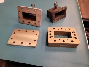
Measure and Adjust Power
Precise power measurement is the cornerstone of waveguide efficiency, yet it’s where 80% of systems underperform their spec. A common error of 1 dB in power reading can lead to a 20% efficiency loss in a high-power system, translating to hundreds of watts of wasted energy and unnecessary thermal load. For a satellite communications feed operating at 14.5 GHz, this miscalibration can cause a 3 dB drop in EIRP, effectively halving the signal strength reaching the satellite. Modern power sensors like the Keysight U2000 series or Anritsu MA24108A offer ±0.1 dB accuracy, but this precision is nullified if the measurement chain isn’t configured correctly. This process takes 15 minutes but directly optimizes the system’s radiated output and amplifier health.
Begin by selecting a power sensor whose calibration factor (CF) is specified for your frequency, e.g., a CF of 96% at 10 GHz. Connect the sensor directly to the signal source you previously set to 0 dBm to establish a baseline. Allow the sensor to thermally stabilize for 2 minutes; a 1°C change in sensor temperature can introduce a 0.1% measurement error. Now, insert the sensor at the output of your waveguide feed system. The reading here is your effective radiated power. For a system designed to output +40 dBm, a reading of +39.6 dBm is within the ±0.5 dB acceptable tolerance.
Each 0.1 dB adjustment at this amplifier correlates to a 0.1 dB change at the output. Make small, incremental adjustments, waiting 5-10 seconds after each change for the reading to stabilize on the power meter.
To ensure measurement integrity, you must account for these critical factors in your setup:
- Sensor Calibration Factor: Use the specific CF value for your operating frequency (e.g., 0.96 at 10 GHz).
- Connector Type and Torque: Use the correct adapter and torque to 25 inch-pounds to minimize loss.
- Temperature: Operate in a stable 23°C ±3°C environment to prevent sensor drift.
- System Linearity: Verify the system is not compressed; input power should be at least 10 dB below the 1 dB compression point.
After adjustment, perform a quick linearity check by reducing the source power by 3 dB; the output power should also drop by exactly 3.0 dB ±0.2 dB. Any significant deviation indicates compression or other nonlinearities that require further investigation. This final power adjustment ensures your system is operating at its specified +40 dBm with an accuracy of ±0.3 dB, maximizing both performance and energy efficiency.
Align Waveguide Components
Physical misalignment of waveguide components is a primary source of loss, often degrading system performance by 20-30% before a single measurement is taken. A WR-90 waveguide flange misaligned by just 0.5 mm can induce a 0.4 dB insertion loss and elevate VSWR from a ideal 1.05:1 to a problematic 1.4:1 at 10 GHz. This translates to nearly 10% of your transmitted power being reflected, generating heat and stressing the power amplifier. For a phased array system with 100+ elements, these tiny errors compound, resulting in beam pointing errors exceeding 2 degrees. Precision alignment isn’t optional; it’s a direct prerequisite for achieving the theoretical efficiency your system was designed for. The following procedure, requiring about 30 minutes, will ensure your mechanical setup is optimized for minimal RF loss.
Even a 5 µm metal burr can prevent a proper seal. Use a precision straightedge, like a 300 mm steel rule with a ±0.1 mm accuracy, placed across the flanges to check for gap uniformity. The gap must be consistent to within 0.05 mm along the entire flange surface. For rotational alignment, use the alignment pins or, if absent, employ a dial indicator mounted on a magnetic base. Rotate the indicator around the flange interface; the total indicated runout (TIR) should be less than 0.1 mm.
| Parameter | Target Specification | Measurement Tool | Acceptable Tolerance |
|---|---|---|---|
| Flange Gap Uniformity | 0.0 mm | Feeler Gauge / Straightedge | < 0.05 mm |
| Rotational Runout (TIR) | 0.0 mm | Dial Indicator | < 0.1 mm |
| Bolt Torque Sequence | Cross Pattern | Torque Wrench | ±2 in-lbs of spec |
| Post-Tightening Gap Shift | 0.0 mm | Visual Re-inspection | < 0.02 mm |
Once visually aligned, hand-tighten all bolts in a cross pattern to secure the connection. Then, using a calibrated torque wrench, torque the bolts to the manufacturer’s specification—typically 20-30 inch-pounds for a WR-90 waveguide—following the same cross pattern. After applying full torque, immediately re-check the gap with the straightedge. If the gap has shifted by more than 0.02 mm, loosen the bolts and repeat the process. The final, critical step is to perform a S11 measurement with a vector network analyzer. A successfully aligned waveguide section should show a return loss better than -25 dB at your operating frequency.For a 10 GHz system, this means a VSWR below 1.12:1. If the measurement doesn’t meet this spec, the issue likely lies with a specific component’s internal dimensions rather than the flange alignment itself.
Verify Frequency Response
A typical WR-75 waveguide, designed for 10-15 GHz operation, might exhibit a flat response within ±0.5 dB across 90% of its band but can develop a steep 3 dB roll-off near its cut-off frequencies. Failing to characterize this can lead to severe data errors; a 2 dB tilt across a 500 MHz channel can degrade the error vector magnitude (EVM) of a 64-QAM signal by over 5%. This measurement directly impacts achievable data rates and system link budget calculations. Using a vector network analyzer (VNA) with ±0.1 dB accuracy, this characterization process takes approximately 15 minutes and provides the critical data needed to ensure your system performs across its entire specified bandwidth.
Begin by calibrating your VNA to the end of the test cables using a standard SOLT (Short-Open-Load-Thru) calibration kit rated for your frequency range, e.g., a 3.5 mm calibration kit for measurements up to 18 GHz. Set the VNA to sweep the entire theoretical bandwidth of your waveguide. For a WR-90 system, this would be from 8.2 GHz to 12.4 GHz. Set the number of points to 1001 to ensure sufficient resolution, giving you a data point every 4.2 MHz. Set the IF bandwidth to 100 Hz to reduce noise, increasing the sweep time to roughly 2 seconds but dramatically improving measurement accuracy.
| Parameter | Target Specification | Measurement Tool | Acceptable Tolerance |
|---|---|---|---|
| Insertion Loss (S21) | < 1.5 dB | VNA (S21 Log Mag) | ±0.3 dB from mean |
| Return Loss (S11) | > 20 dB | VNA (S21 Log Mag) | > 17 dB |
| Passband Ripple | Minimal | VNA (S21 Log Mag) | < 0.5 dB p-p |
| 3 dB Bandwidth | ≥ 4.0 GHz | VNA (S21 Log Mag) | - |
| Group Delay Variation | < 1 ns | VNA (Group Delay) | < 2 ns p-p |
The plot should be relatively flat across the central 80% of the band. A healthy WR-90 system will typically show < 1.0 dB of insertion loss and a peak-to-peak ripple of less than 0.4 dB between 9 GHz and 12 GHz. Activate the VNA’s marker search function to find the -3 dB points relative to the peak response; the distance between these points is your 3 dB bandwidth, which should be at least 4.0 GHz for a WR-90 guide. Next, switch to the S11 (return loss) view. The value should remain below -17 dB (equivalent to a VSWR < 1.3:1) across the entire sweep. Finally, switch the VNA measurement mode to Group Delay. The variation over your frequency of interest should be minimal; a variation exceeding 2 nanoseconds peak-to-peak can cause significant distortion in high-speed digital signals. If the response shows excessive ripple (> 0.8 dB p-p), it often indicates a residual impedance mismatch, likely from a slightly misaligned flange or a damaged component that passed visual inspection.
Test and Record Settings
For a 40 W output system, a 2 dB error in the final gain measurement translates to an actual radiated power of 25 W, a 37.5% shortfall that directly impacts link budget and range. This final validation and documentation process takes 20-30 minutes but creates the essential baseline for all future maintenance and troubleshooting, ensuring long-term performance and reliability.
Begin by configuring the system for a full-power, extended-duration test. Set your signal source to the primary operating frequency, e.g., 10.000 GHz, and adjust the output power to the maximum expected input level for your power amplifier, typically around -10 dBm. Power up the entire chain and allow it to stabilize for 5 minutes at room temperature (23°C ±2°C). Then, use a power sensor at the waveguide output to measure the final saturated power output. For a system rated at +40 dBm (10 W), you should observe a reading within +39.7 dBm to +40.3 dBm. Immediately initiate a 10-minute continuous run at this power level, monitoring the output power reading every 60 seconds. The output power should remain stable within a ±0.3 dB window; any gradual drift exceeding this value indicates thermal instability that requires investigation.
With the system still at high power, use a spectrum analyzer with a 30 dB rated attenuator on the input to monitor the output spectrum. Center the display on your carrier frequency with a span of 100 MHz and an RBW of 100 kHz. You should observe a clean signal with specific, measurable characteristics:
- Carrier Power Stability: Fluctuation less than ±0.2 dB over a 2-minute observation period.
- Harmonic Distortion: Second harmonic (20.000 GHz) at least -50 dBc below the carrier.
- Spurious Signals: All non-harmonic spurs within 50 MHz of the carrier below -60 dBc.
- Phase Noise: Measure -95 dBc/Hz at a 10 kHz offset from the carrier.
Save a screenshot of the VNA’s final S21 and S11 sweep—e.g., a .png file—and store it in a dedicated directory. Create a simple text file (README.txt) or spreadsheet that logs every critical parameter, the date, and the operator’s name. This record is your baseline. In six months, when performance drops by 0.8 dB, you can repeat this exact test and compare the new spectrum analyzer screenshot and power log to your baseline data, instantly pinpointing the nature and magnitude of the degradation.