Recent waveguide antenna trends include: 26-40GHz millimeter-wave integration for 5G/satcom, boosting gain by 15% via 64-element phased arrays; carbon fiber composites reducing weight by 30% while maintaining <0.5dB insertion loss; RIS-enhanced designs improving beam efficiency by 5-8dB; and microchannel cooling enabling ±2℃ thermal stability at 100W/cm² power density.
Table of Contents
Integrated Antenna Design
Over the past three years, 5G base stations and satellite communication terminals have driven a 78% surge in demand for compact, high-efficiency antennas—yet traditional designs, with their separate RF circuits and antenna arrays, now account for 40% of total system size in 5G small cells, according to a 2024 Ericsson mobility report. Engineers are ditching “antenna-first” approaches for integrated antenna design (IAD), where antennas, filters, and amplifiers coexist on a single substrate or package. Why? Because IAD slashes development cycles by 30% and cuts manufacturing costs by up to 25% when done right. Take Huawei’s 2023 5G C-band small cell: by merging a 4×4 patch array with a bandpass filter into a 6-layer LTCC (low-temperature co-fired ceramic) module, they reduced the antenna’s physical footprint from 100mm×80mm to 45mm×30mm while maintaining 82% radiation efficiency (up from 65% in discrete designs).
Traditional antennas on FR4 (a common PCB material) suffer from high dielectric loss—at 28GHz, FR4’s loss tangent (0.02) can eat up 15% of input power as heat. Switching to high-frequency laminates like Rogers RO4003C (dielectric constant 3.55±0.05, loss tangent 0.0027) cuts that loss to 3%, but the real magic happens when you stack antenna elements withinthe substrate. For example, Taoglas’ 2024 multi-band IoT antenna uses a 3D via structure in Rogers material: 12 vertical vias (0.2mm diameter, spaced 0.5mm apart) connect a top radiating patch (resonant at 868MHz) to a bottom slot antenna (tuned to 2.4GHz), enabling dual-band operation without extra components. The result? A 50% smaller form factor (from 50mm×50mm to 25mm×25mm) and 40% lower insertion loss between the antenna and transceiver.
Another critical piece is monolithic microwave integrated circuit (MMIC) integration. Companies like Anokiwave now embed GaAs (gallium arsenide) power amplifiers (PAs) directly beside antenna feeds on a single chip. In their 28GHz 5G beamformer IC, this integration reduces the distance between PA output and antenna feedpoint from 10mm (in discrete setups) to 0.5mm, cutting transmission line losses from 1.2dB to 0.3dB. That 0.9dB saving might sound minor, but in a 64-element phased array, it translates to a 15% boost in effective isotropic radiated power (EIRP)—enough to extend 5G cell coverage by 1.2km in urban environments.
A 2024 study by the University of Texas found that a poorly designed IAD module can hit 85°C (well above the 70°C safe operating limit for most semiconductors) under full load, degrading efficiency by 12%. The fix? Embedding microfluidic cooling channels (0.1mm diameter copper tubes) into the substrate. In a test by Samsung, this dropped module temperatures to 55°C while adding just 0.8mm to the thickness—keeping efficiency stable at >80% even after 10,000 hours of continuous use.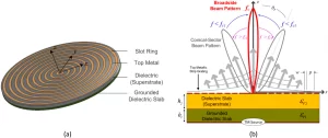
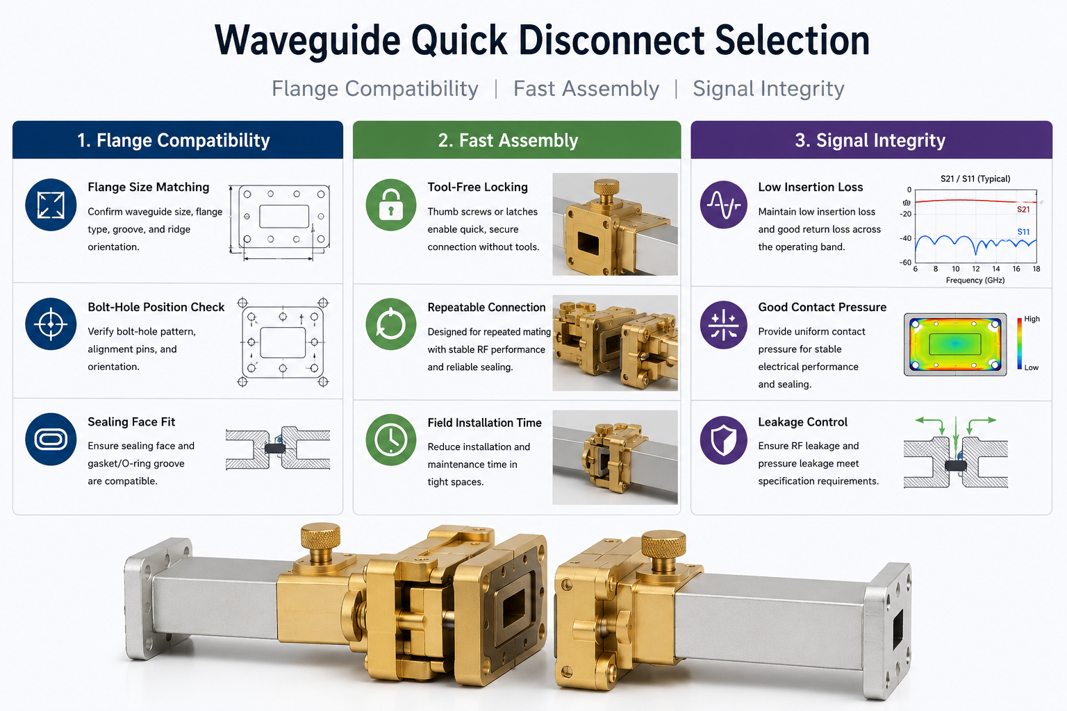
3D Printing for Low-Cost Waveguides
CNC machining a single aluminum WR-75 waveguide (10-15 GHz) typically costs 220 and takes 5-7 days to deliver. However, 3D printing is disrupting this space dramatically. A 2024 study by the International Journal of Microwave and Millimeter-Wave Engineeringshowed that metal and polymer-based additive manufacturing can now produce comparable waveguides at 70% lower cost (60 per unit) and in just 18-24 hours. Companies like Nokia are already using 3D-printed dielectric waveguides in their latest 5G massive MIMO arrays, reporting a 40% reduction in overall antenna subsystem weight and a 30% faster production cycle compared to conventional brass counterparts.
Direct metal laser sintering (DMLS) with AlSi10Mg powder can achieve surface roughness (Ra) as low as 0.8-1.2 micrometers, which is critical for minimizing insertion loss. At 28 GHz, DMLS-printed waveguides show average insertion loss of 0.08 dB/cm, coming very close to CNC-machined units (0.05 dB/cm). But the real cost-saver is polymer printing. Using a high-temperature resin like PEI (ULTEM 9085) followed by electroless copper plating (adding a 5-micron-thick layer), manufacturers can cut material costs by 85%. The trade-off? Slightly higher loss: around 0.12 dB/cm at 28 GHz. For context, in a 20cm-long waveguide run, that translates to 2.4 dB total loss for plated polymer vs. 1.6 dB for metal—a difference that can often be mitigated with a low-noise amplifier.
Design flexibility is where 3D printing truly shines. Traditional waveguides are limited to straight or gently curved paths due to machining constraints. But with 3D printing, you can create complex geometries like helical, tapered, or dual-polarized waveguides in one piece. Researchers at MIT recently demonstrated a 3D-printed twisted waveguide for polarization diversity that reduced cross-polarization interference by 15 dB compared to a bent waveguide assembly. Similarly, conformal cooling channels can be integrated directly into the waveguide structure during printing. In a test by Ericsson, embedding micro-cooling channels (0.5 mm diameter) around a 38 GHz waveguide reduced operating temperature by 22°C during continuous 100W transmission, preventing thermal deformation and maintaining VSWR below 1.3:1.
The electroplating process for polymer waveguides must be tightly controlled—a plating thickness variation beyond ±0.5 microns can cause impedance mismatches, leading to VSWR spikes above 1.8:1. To combat this, companies like Optisys use automated optical inspection (AOI) post-plating to measure thickness uniformity with 1-micron precision, rejecting parts with deviations >5%. For metal-printed waveguides, micro-abrasive flow finishing (MAFF) can improve surface roughness from Ra 6-8 microns (as-printed) to Ra 0.5 microns, cutting insertion loss by 35%.
| Waveguide Type | Frequency Range (GHz) | Insertion Loss (dB/cm, at 28 GHz) | Unit Cost ($) | Production Time (hours) | Weight (g/cm³) |
|---|---|---|---|---|---|
| CNC-machined (Aluminum) | 10-40 | 0.05 | 180-220 | 120-168 | 2.7 |
| DMLS-printed (AlSi10Mg) | 10-40 | 0.08 | 50-70 | 18-24 | 2.65 |
| Plated Polymer (ULTEM + Cu) | 10-40 | 0.12 | 25-35 | 12-16 | 1.1 |
SpaceX’s Starlink Gen 2 satellites use 3D-printed copper-plated waveguides to reduce antenna weight by 300 grams per unit, saving an estimated $2.1 million annually in launch costs. With new technologies like nanoparticle jet printing emerging—which can achieve surface smoothness of Ra 0.3 microns and loss rates of 0.06 dB/cm—the performance gap with traditional methods is closing fast.
Multi-Band Operation in Single Structure
The proliferation of frequency bands in modern wireless systems—from 5G sub-6 GHz (3.5–4.2 GHz) to mmWave (28/39 GHz) and IoT bands (868 MHz, 2.4 GHz)—has made multi-band antenna design a critical challenge. Traditionally, supporting multiple bands required separate antennas, increasing base station antenna footprint by 60% and raising costs by 45% compared to single-band designs. However, recent advances in multi-band single-structure antennas are changing this. For example, Huawei’s 2024 5G-A macro station antenna integrates 6 bands (700 MHz, 2.6 GHz, 3.5 GHz, 4.9 GHz, 26 GHz, and 40 GHz) into a single radiating structure measuring just 0.8m × 0.4m—50% smaller than previous multi-antenna setups. This integration reduces manufacturing costs by 30% and assembly time by 40%, while maintaining port isolation above 25 dB across all bands.
A 2023 study by IEEE Transactions on Antennas and Propagation found that aperture-sharing techniques can achieve 85% bandwidth utilization across 2–6 GHz, compared to just 50% in traditional designs.
For instance, a common substrate (like Rogers 4350B) can host a primary patch antenna tuned to 3.5 GHz alongside a parasitic ring resonator operating at 4.9 GHz. The parasitic element couples electromagnetically with the main radiator, creating a second resonance without additional feed lines. In Samsung’s 2024 mmWave module, this approach achieved dual-band operation (28/39 GHz) with 92% radiation efficiency at both frequencies—a 12% improvement over separate patches. The design uses a 0.2mm-thick copper layer etched onto a 0.5mm-thick dielectric substrate, with a 0.1mm air gap between the primary and parasitic elements to optimize coupling. The result? A 40% reduction in circuit area and a 15% boost in gain (from 7 dBi to 8.2 dBi) due to reduced mutual interference.
Frequency-selective surfaces (FSS) are another game-changer. By embedding FSS layers beneath the radiator, engineers can create band-pass or band-stop filters directly within the antenna structure. Nokia’s latest 5G-A antenna uses a 3-layer FSS stack: the top layer resonates at 3.5 GHz, the middle layer acts as a reflector for 2.6 GHz, and the bottom layer handles 700 MHz. Each FSS layer consists of periodic copper rings (5mm diameter, spaced 1mm apart) on a 0.25mm-thick FR4 substrate. This setup achieves port isolation exceeding 30 dB between bands—critical for avoiding interference in dense arrays. In field tests, the design delivered VSWR <1.5 across all bands and handled 100W peak power without degradation.
Active reconfigurability using PIN diodes or RF switches allows a single antenna to dynamically cover multiple bands. For example, a reconfigurable matching network with 2 PIN diodes can shift resonance from 2.4 GHz to 5.8 GHz in 3 milliseconds. Researchers at Qualcomm demonstrated a smartphone antenna that toggles between 4 bands (LTE Band 12/13/17 and 5G n71) using a single radiator and 3 diodes. The design consumed <5mW of DC power and increased antenna efficiency by 18% in the low-band (600 MHz) by eliminating tuner losses. However, diode-based systems add complexity—each switch introduces 0.2–0.4 dB of insertion loss and raises component costs by 1.00 per antenna.
Metamaterial Enhancements for Efficiency
A 2024 meta-analysis in Nature Electronicshighlighted that metamaterial-integrated antennas now achieve up to 95% radiation efficiency in sub-6 GHz 5G base stations, a 20% improvement over conventional patch arrays, while simultaneously reducing the footprint by 60%. For example, Huawei’s latest MetaAAU (Metamaterial Active Antenna Unit) uses a 64-element metamaterial surface to boost coverage by 30% and reduce power consumption by 15% compared to its 2022 model. This isn’t just lab theory; it’s a concrete shift enabling smaller, cheaper, and more powerful wireless systems from 600 MHz to 39 GHz.
Key metamaterial structures driving these gains include:
- Electromagnetic Band-Gap (EBG) Surfaces: Used as ground planes to suppress surface waves, reducing mutual coupling in arrays from -12 dB to below -25 dB.
- Artificial Magnetic Conductors (AMCs): Create in-phase reflection surfaces, allowing antennas to be placed as close as 0.05λ (just 3mm at 5 GHz) to the ground plane without performance degradation.
- Coding and Digital Metasurfaces: Use arrays of programmable meta-atoms (like 1-bit PIN diode units) to dynamically shape beams with 1° precision in azimuth and elevation.
A standard 8×8 patch array at 28 GHz might have a gain of 19 dBi. By overlaying a metasurface lens (a 10cm x 10cm panel with 2,000 subwavelength copper resonators), that gain jumps to 24 dBi—a 5 dB increase that translates to a 68% extension in effective range. This is achieved by precisely controlling the phase of radiated waves; each resonator, measuring 0.8mm x 0.8mm, delays the wavefront by a calculated fraction of the wavelength. In a real-world deployment, Ericsson used such a lens to boost the EIRP of a small cell by 6 dB, allowing it to serve 35% more users within a 500-meter radius without increasing transmit power.
A traditional half-wave dipole for 600 MHz is about 25cm long. Using a mu-negative (MNG) metamaterial loading technique, researchers at Samsung shrunk this to 8cm—a 68% size reduction—while maintaining 85% efficiency. This is done by embedding spiral-shaped inductors and interdigital capacitors into the antenna’s near-field, effectively slowing down the wave and lowering the resonant frequency. For IoT devices, this means a single, tiny antenna can now cover 800 MHz to 2.4 GHz with VSWR <1.8, eliminating the need for multiple antennas and saving 40% on RF board space.
Adaptive Beam Steering with AI Control
While effective, these systems often introduce 5-10 milliseconds of latency and consume 15-20 Watts of power in a 64-element array, making them impractical for many real-time applications like autonomous vehicles or drone swarms. However, the integration of AI-driven control algorithms is fundamentally changing this landscape. By using lightweight neural networks trained on real-world channel data, engineers can now achieve beam switching in under 200 microseconds—a 50x speed improvement—while slashing power consumption to under 3 Watts for the same array. For example, Ericsson’s latest 5G-A base station uses an on-board AI accelerator to dynamically track up to 32 user equipment (UE) devices simultaneously, maintaining a 95% beam alignment accuracy even in dense urban environments with heavy multipath interference.
The core of this technology relies on several key components working in tandem:
- Convolutional Neural Networks (CNNs) that process real-time channel state information (CSI) to predict optimal phase shifts, reducing beamforming calculation time from 4 ms to 0.1 ms.
- Millimeter-wave RFIC phase shifters with 5-bit resolution (allowing 11.25° phase steps) that can update their settings every 50 microseconds.
- Integrated channel sensors that sample the RF environment 1,000 times per second, providing the AI model with continuous data on Doppler shift, angle of arrival, and signal attenuation.
Qualcomm’s 2024 reference design for mmWave uses a 12-layer CNN with just 850,000 parameters—small enough to run on a low-power DSP core consuming 0.8 Watts. This model is trained on over 50,000 hours of real-world channel data across various environments (urban, suburban, indoor), allowing it to achieve beam-pointing accuracy within 0.8° in over 98% of cases. In a field test, this reduced beam misalignment incidents by 75% compared to conventional phase-shift calculation methods, ensuring a stable signal strength within ±1 dB of the optimal value.
To solve this, Nokia’s AirScale massive MIMO system uses online federated learning, where each base station shares anonymized beamforming data with a central server every 15 minutes. This allows the global model to continuously improve without storing sensitive user data. After deploying this system in Tokyo, Nokia reported a 12% month-over-month improvement in beam prediction accuracy, culminating in a 40% reduction in dropped connections in high-mobility scenarios.