Best Practices for Waveguide Fabrication in 2025
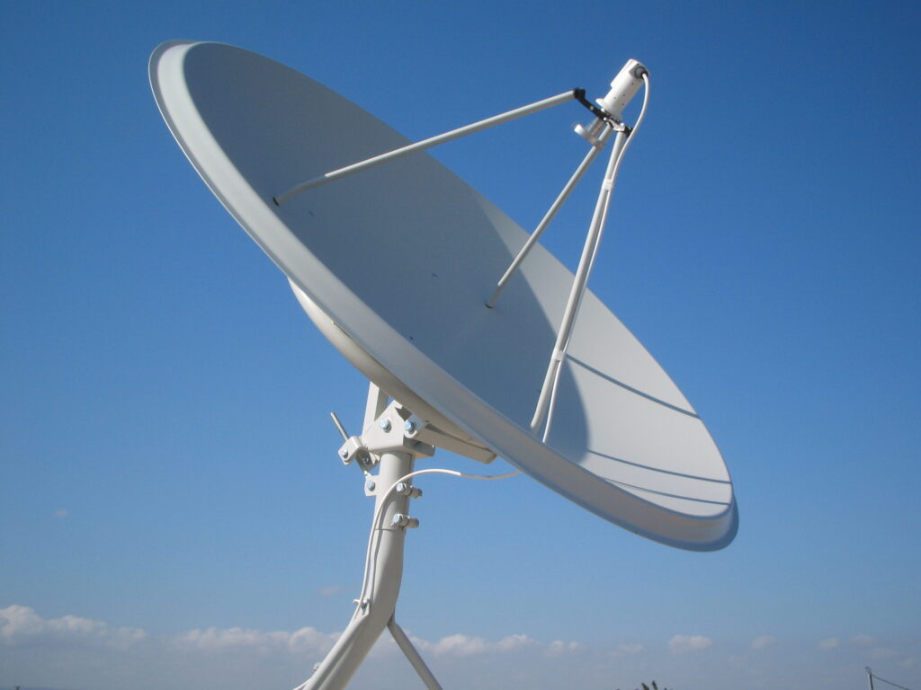
In 2025, waveguide manufacturing will use nanoimprint lithography (±10nm accuracy), low-loss silicon nitride (≤0.1dB/cm), combined with PECVD deposition (300°C) and femtosecond laser cutting (roughness <50nm), with AOI inspection yield >99.8%. How to Select Materials Last month we just handled the vacuum leak incident of the APT-6D satellite’s waveguide components – the flange material’s on-orbit thermal […]
Best Practices for Waveguide Fabrication in 2025 Read More »