By precisely controlling return loss below -10dB, customized antennas significantly enhance signal transmission efficiency by 20% within a miniature size and effectively reduce system power consumption by 15%, thereby ensuring superior connectivity stability and authoritative reliability for multi-band connections in complex industrial environments.
Table of Contents
Power Efficiency
Through precise impedance matching, customized antennas control the Voltage Standing Wave Ratio (VSWR) between 1.2 and 1.5, making the return loss better than -15dB.
This design allows the RF front-end to reduce the current from 120mA to approximately 85mA under the same transmit power.
In actual NB-IoT or LoRaWAN testing, this efficiency improvement can extend the operating life of a device with a 2500mAh battery from 3.5 years to over 5 years, with radiation efficiency stabilizing between 70% and 85%.
Radiation Efficiency Comparison
Common standard ceramic antennas, PCB trace antennas, Flexible Printed Circuit (FPC) antennas, and customized 3D structured antennas (such as LDS) on the market exhibit vastly different performance in the same frequency band.
Standard chip ceramic antennas typically use high-dielectric-constant ceramic substrates to pursue miniaturization, which leads to narrower radiation bandwidth and increased loss; their radiation efficiency usually stays between 25% and 40%.
In contrast, customized FPC antennas designed for specific housing environments can increase efficiency to 65% – 75% by optimizing the radiator area and bracket height.
For IoT devices that need to pass carrier certifications, this efficiency difference directly determines whether a product can be launched.
The table below lists typical measured data comparisons for several mainstream antenna solutions under North American LTE-M bands (e.g., Band 12, 700MHz) and European NB-IoT bands (e.g., Band 20, 800MHz):
| Antenna Type | Typical Size (mm) | Radiation Efficiency (Typical) | Peak Gain (dBi) | Return Loss (S11) | System TRP Performance (dBm) |
|---|---|---|---|---|---|
| Standard Miniature Ceramic Chip | 3.2 x 1.6 x 1.1 | 22% – 35% | -1.5 to 0.5 | -6dB to -8dB | 14.5 to 16.5 |
| 1.6mm FR4 PCB Custom | 40 x 15 (Clearance) | 50% – 60% | 1.0 to 2.2 | Below -10dB | 17.5 to 19.0 |
| 50um PI Substrate FPC | 35 x 12 (Attached) | 65% – 75% | 2.5 to 3.5 | Below -15dB | 19.5 to 21.0 |
| Custom LDS (3D Plastic) | Depending on Housing | 70% – 82% | 3.0 to 4.2 | Below -18dB | 20.5 to 22.0 |
In the Sub-GHz frequency band, the antenna actually works in coordination with the entire PCB; the PCB acts as the other half of the antenna.
If the length of the PCB is less than one-quarter of the signal wavelength, the radiation efficiency will decay rapidly as the ground plane decreases.
Experimental data shows that when the PCB length is reduced from 100mm to 40mm, the efficiency of a standard 868MHz antenna drops from 65% to below 20%.
Customized designs can compensate for this impedance mismatch caused by insufficient ground planes by adding parasitic elements or adjusting the feed structure, bringing the efficiency back to over 45%.
The loss tangent of standard FR4 material is around 0.02, while Polyimide (PI) or high-performance composite materials commonly used in customized antennas can reduce this value to 0.003.
In high-frequency applications such as 2.4GHz or 5GHz, this material difference leads to a radiation loss of 1dB to 2dB.
In actual link testing, a 2dB efficiency improvement allows the device to gain about 20% more coverage distance in the same transmission environment, or reduce the transmit current by about 30mA at the same distance.
The table below shows the details of energy loss for different materials and processes in a 2.4GHz Wi-Fi/Bluetooth environment:
| Material & Process | Relative Permittivity (Dk) | Loss Tangent (Df) | Antenna Thermal Loss (dB) | Final Radiation Efficiency |
|---|---|---|---|---|
| Ordinary FR4 Printing | 4.4 | 0.02 | 1.8 | 45% – 55% |
| High-Frequency Rogers Substrate | 3.5 | 0.004 | 0.4 | 80% – 88% |
| Polyimide (FPC) | 3.2 | 0.008 | 0.7 | 70% – 78% |
| Laser Direct Structuring (LDS) | 3.0 | 0.005 | 0.5 | 75% – 85% |
For LoRa gateways or sensors operating in the field, improving receiving sensitivity from -135dBm to -138dBm often relies on this 3dB of antenna efficiency.
If an antenna with an efficiency of only 30% is used, the RF chip must frequently switch to high-gain mode to maintain the connection, which generates an additional 50mW to 80mW of power consumption.
By using a customized antenna with an efficiency of 75%, the signal strength received is sufficient to allow the chip to stay in a low-power listening state for long periods.
In designs where multiple frequency bands coexist, such as vehicle trackers with GPS, LTE, and Wi-Fi, the isolation between antennas also interferes with efficiency.
If the antenna layout is unreasonable, energy will couple to adjacent antennas and be consumed as heat; this mutual coupling loss can sometimes be as high as 3dB.
Customized solutions can optimize the isolation between antennas from -10dB to below -20dB by adjusting the polarization direction of the antenna radiator and setting spatial notch filters, ensuring that each band achieves a radiation efficiency of over 60%.
Reducing Retransmission Frequency
Through customized antenna solutions, an additional 3dB to 6dB of link budget gain can be stably obtained. In the RF field, a 3dB improvement manifests as a doubling of spatial signal power.
When devices are located in basements, metal enclosures, or the weak signal coverage edges of North American suburbs, these few decibels of gain can reduce the Packet Error Rate (PER) from over 15% to below 1%.
Due to the reduction in Automatic Repeat Requests (ARQ) repeatedly triggered at the MAC layer (Media Access Control layer), the effective energy utilization of the battery has been substantially improved.
- Energy Efficiency Loss of Coverage Enhancement Mechanisms: NB-IoT or Cat-M1 protocols have built-in Coverage Enhancement (CE) levels. In environments with poor signal quality, the protocol will force entry into CE Level 2 mode, repeatedly sending each uplink packet up to 128 times. If the antenna efficiency is increased by 5dB, the device can stay in CE Level 0 state, requiring only 1 transmission to complete communication. The power consumption gap between the two is more than a hundredfold.
- Improvement of Signal-to-Noise Ratio (SNR): Customized antennas effectively filter out non-coherent noise in the environment through optimized polarization matching and radiation patterns. In crowded bands such as 2.4GHz, increasing the SNR by 4dB can significantly improve the decoding success rate of Orthogonal Frequency Division Multiplexing (OFDM) signals, thereby avoiding link reconnections caused by CRC (Cyclic Redundancy Check) errors.
- Reducing Peak Current during Network Search: When antenna gain is insufficient to maintain a stable base station connection, the device will frequently drop offline and enter a high-power network search mode.
Because standard antennas cannot adapt to the PCB ground plane size of specific products, they often lead to return loss degradation to around -6dB, where a large amount of energy is reflected back to the RF chip at the antenna feed point and converted into heat.
Through customized development, the return loss can be precisely controlled below -15dB, making the Voltage Standing Wave Ratio (VSWR) reach an excellent level of 1.25.
This precise matching state ensures that every milliwatt of energy output by the power amplifier is radiated into the air as much as possible.
In scenarios where sensors periodically upload data, the milliampere-hour (mAh) consumption of a single communication cycle is reduced by 30% to 45%, allowing devices that originally required two AA batteries to achieve the same operating cycle with a single battery.
- Multipath Fading Compensation Performance: In urban building environments, signals reach the receiving end through multiple reflections, which easily causes deep fading phenomena. Customized antennas can reduce the probability of signal cancellation at specific spatial positions through dual-antenna diversity technology or by changing polarization methods, reducing handshake failures at the physical layer due to instantaneous disconnection.
- Avoidance of Buffer Overflow: Frequent retransmissions cause backlogs in the device’s internal transmit buffer, forcing the processor (MCU) to stay out of low-power sleep mode while waiting. Maintaining a high single-transmission success rate allows the MCU to quickly process protocol stack tasks and turn off peripheral power, achieving system-level power saving.
- Stability in Dynamic Environments: Many IoT devices are installed on vehicles or around the human body, where environmental loads are in a state of change. Customized antennas are simulated using human body models (Phantom) or metal structures during the design phase to ensure that the antenna frequency does not shift in these complex environments. In contrast, the resonant frequency of standard antennas may shift by more than 50MHz when close to the human body, causing an instantaneous loss of 10dB in the link budget and inducing large-scale packet retransmissions.
By optimizing the Total Radiated Power (TRP) of the antenna to over 20dBm and maintaining a radiation efficiency of over 70% in the low-frequency bands of 700MHz to 900MHz, the time the device spends in a high-current emission state can be significantly shortened.
Experimental data shows that when the Received Signal Strength Indicator (RSSI) is optimized from -115dBm to -108dBm, the increase in data throughput indirectly reduces the online time of the wireless circuit.
In typical NB-IoT applications, every decibel of link margin added can save considerable battery Coulomb capacity over a ten-year lifespan, providing a reliable physical foundation for the long-term low-cost operation of the entire IoT system.
Ultra-Compact Size
In modern IoT devices, ultra-compact solutions compress the antenna footprint to below 5mm x 5mm.
By utilizing high-dielectric-constant media (Dk 10-20), physical dimensions can be reduced by 40%.
For the 2.4GHz band, customized designs achieve an average gain of over -2dBi with 1mm clearance and return loss below -10dB, ensuring stable CAT-M1 and NB-IoT links and keeping the overall terminal thickness within 8mm.
Spatial High Integration Technology
This process uses thermoplastic plastics containing metal oxide additives, such as PC/ABS or modified PPA, and performs surface activation on the bracket surface according to a preset path using a 1064nm laser.
In the subsequent electroless plating stage, metal particles are deposited in the activated area, forming a conductive layer 12 to 15 microns thick, covering a 2 to 4 micron nickel layer and a 0.1 micron gold layer.
The antenna adheres to the geometric contour of the bracket without occupying additional physical volume, achieving zero-incremental space allocation.
In the 2.4GHz band, this solution utilizes irregular surfaces to increase the effective radiation path by 20%, keeping the return loss below -10dB within a 100MHz bandwidth.
Compared to the 0.5mm assembly tolerance of traditional metal shrapnel antennas, this processing precision is controlled within plus or minus 0.05mm, reducing resonant frequency shifts between production batches.
- LDS Process Parameters: Laser power is set between 5W and 10W, and scanning speed reaches 2000mm/s to 4000mm/s, ensuring the plastic substrate does not undergo thermal deformation.
- Plating Thickness Indicators: The copper layer thickness is no less than 10 microns to ensure low loss, the nickel layer provides hardness support, and the gold layer ensures low contact resistance at the RF feed point, with typical values less than 50 milliohms.
- Frequency Coverage Range: Supports signals from low-frequency NB-IoT at 600MHz to the WiFi 6E band at 6GHz; a single bracket can accommodate 3 to 5 independent antenna arrays.
Flexible Printed Circuit (FPC) integration solutions perform excellently in thickness control, with the total thickness of standard double-layer FPCs maintained at 0.12mm to 0.15mm.
The substrate is chosen from Polyimide (PI) or low-loss Liquid Crystal Polymer (LCP), where LCP exhibits excellent dielectric stability in 28GHz environments, with a loss tangent (Df) below 0.003.
FPC antennas are attached via adhesive to non-metallic support surfaces inside the device, such as plastic mid-frames or battery covers.
In extremely compact smart wearable devices, the vertical clearance between the antenna radiation unit and the battery foil is often compressed to 0.2mm to 0.5mm.
To reduce inductive eddy current loss caused by metal battery foil, a flexible ferrite sheet with a thickness of 0.05mm and an initial magnetic permeability between 50 and 100 is added between the FPC and the battery.
This structure effectively guides magnetic field lines in the 13.56MHz NFC band or sub-6GHz cellular bands, increasing radiation efficiency from 15% to over 35%.
In multi-band LTE deployments, FPC solutions support the integration of the 700MHz low-frequency band and 2700MHz high-frequency band with coaxial feeding, achieving multi-resonance characteristics through precisely calculated bifurcated paths.
- Bending Reliability: Supports 180-degree folding with a radius of 0.5mm; after 1000 bending cycles, the resistance drift of the metal traces is less than 5%.
- Dielectric Constant Control: The Dk value of the LCP substrate is stable at around 2.9, reducing antenna center frequency drift caused by environmental humidity changes, with a temperature drift coefficient of less than 50ppm.
- Clearance Allocation Data: By side-mounting the FPC on the edge of a PCB with a total area of 400 square millimeters, the ground plane isolation can be increased to over 15dB.
For applications in the millimeter-wave band (24GHz to 60GHz), Antenna-in-Package (AiP) technology integrates radiation units directly into the semiconductor package.
This approach eliminates signal attenuation caused by long-distance traces between the RF chip and the antenna.
At a frequency of 28GHz, every centimeter of traditional PCB trace generates about 1dB of insertion loss, whereas the interconnect length of the AiP structure is shortened to the micron level.
Packaging materials use Low Temperature Co-fired Ceramic (LTCC) or Redistribution Layer (RDL) technology, with the dielectric constant of LTCC controlled between 5.9 and 9.0.
By arranging 2×2 or 4×4 microstrip array antennas on the packaging substrate, a high directivity gain of 8dBi to 12dBi is achieved, cooperating with phase shifter chips to complete beam scanning of plus or minus 45 degrees.
The size of RF front-end modules typically does not exceed 10mm x 10mm x 1.5mm, and they are mounted on the main PCB, simplifying the design of the entire RF link.
In extremely small clearance environments, the antenna impedance often deviates from the center region, exhibiting high inductive or capacitive reactance.
Using electromagnetic simulation software for full-wave analysis allows for the determination of matching points on a Smith Chart.
Hardware implementation uses lumped elements in 01005 packaging to form multi-stage matching networks, with the precision of inductor values reaching 0.1nH.
Within a 5mm x 5mm PCB reserved area, by optimizing the shape of the Ground Cutout, near-field distribution energy is concentrated around the radiator, reducing electromagnetic interference to other high-speed signal lines on the motherboard.
In actual tests for the NB-IoT band, this layout solution stabilizes the Total Radiated Power (TRP) above 18dBm while meeting the -115dBm receiving sensitivity, ensuring communication quality in environments such as basements or closed metal cabinets.
- Impedance Matching Tolerance: The correlation between electromagnetic simulation and actual measurement must reach over 90%, with the target VSWR value set below 2.0.
- Isolation Optimization: In WiFi and Bluetooth coexistence systems, by inserting Parasitic Elements within a 2mm spacing, additional zeros can be generated, increasing isolation from 10dB to 22dB.
- Thermal Stability Assessment: Under full-load power emission at 85 degrees Celsius, the capacitance variation rate of ceramic capacitors in the matching circuit must be controlled within 5%.
LDS or FPC solutions must pass a 48-hour neutral salt spray test to ensure no corrosion or peeling of the metal plating, with contact resistance change less than 50 milliohms.
After undergoing high and low temperature cycle tests from minus 40 degrees Celsius to plus 85 degrees Celsius, frequency drift caused by thermal expansion and contraction of materials must be controlled within 0.5% of the center frequency.
For mass production, automated AOI (Automated Optical Inspection) combined with RF coupling testers can complete VSWR detection for a single device within 2 seconds, identifying tiny geometric deformations caused by injection molding stress or laser energy fluctuations.
When there are many metal shields, stainless steel screws, or high-density battery packs inside the device, the near-field distribution of the antenna will undergo severe distortion.
By introducing distributed multi-point grounding technology, a stable reference potential can be established at the PCB edge, reducing stray radiation generated by ground current loops.
When designing 4×4 MIMO antennas for the 5G Sub-6GHz band, using spatial orthogonality to arrange radiation units can reduce the Envelope Correlation Coefficient (ECC) to below 0.1, even within a mobile phone-sized frame with a width of only 70mm.
This low-correlation design supports the stable operation of high-order modulation modes (such as 256QAM), increasing the download rate in weak signal edge areas by over 30%.
Quantitative Comparison of Size Efficiency
According to the Chu-Harrington Limit, when the maximum geometric dimension of an antenna is significantly smaller than 1/2π of its operating wavelength, its quality factor (Q value) will rise exponentially as volume decreases, leading to sharp bandwidth narrowing and increased internal loss.
For IoT devices working in the 2.4GHz band, the free-space wavelength is about 125mm, and the length of a standard quarter-wave monopole antenna is about 31mm.
To integrate such an antenna into a miniature package smaller than 10mm * 10mm * 5mm, it must be achieved through folded paths, loading high-dielectric-constant media, or introducing lumped compensation elements.
Through quantitative testing, it was found that when the envelope volume of the radiator is compressed from 500 cubic millimeters to 50 cubic millimeters, antenna efficiency typically drops from 65% to around 15%.
To maintain communication link stability, engineering usually requires controlling return loss below -10dB, which demands matching networks use inductors with 0.1nH tolerance and capacitors with 0.1pF tolerance to offset strong capacitive impedance deviations caused by size reduction.
| Antenna Technology Solution | Total Occupied Volume (mm^3) | 2.4GHz Efficiency (%) | 5.8GHz Efficiency (%) | Typical Gain (dBi) | Relative Bandwidth (%) |
|---|---|---|---|---|---|
| Standard PCB Inverted-F | 350 | 55 – 60 | 65 – 70 | 1.5 – 2.5 | 12 |
| Ultra-thin FPC Patch | 120 | 35 – 45 | 45 – 55 | -0.5 – 1.0 | 8 |
| Custom LDS 3D Bracket | 200 | 45 – 55 | 55 – 60 | 0.0 – 1.5 | 10 |
| High-Alumina Ceramic Miniature Patch | 25 | 20 – 25 | 30 – 35 | -4.0 – -2.5 | 3 |
| Antenna-in-Package (AiP) | 8 | Not Covered | 40 – 50 | -5.0 – -3.0 | 5 |
When physical volume is compressed to less than 1/15 of the wavelength, radiation resistance will drop below 5 ohms.
In this case, matching circuit loss may exceed the antenna’s own radiated power.
It is recommended to prioritize composite media loading solutions within a 100mm^3 space.
For ceramic patch antennas, although the radiator itself is only 3.2mm * 1.6mm, its bottom and surroundings usually require a metal ground plane clearance area of at least 4mm * 8mm to form a complete electric dipole radiation mode.
If the clearance area is forcibly compressed from 32 square millimeters to 10 square millimeters, it will cause a precipitous drop of 15% to 20% in antenna efficiency.
In contrast, solutions using the device’s plastic housing for LDS processing, although occupying a larger projected area for antenna traces, have about 30% less dependence on internal PCB clearance because they are on the outermost layer and distributed in 3D.
In extremely compact scenarios like smartwatches, using the metal frame as part of the radiator can increase the effective radiation volume to over 1000 cubic millimeters without adding extra volume, thereby maintaining the gain in the Sub-6GHz band above -1dBi and meeting carrier TRP test standards for mobile terminals.
- Space Efficiency Indicator: Defined as the product of gain and bandwidth achieved per unit volume. In a 10mm * 10mm area, the space efficiency of the LDS solution is about 1.8 times higher than that of traditional patch solutions.
- Resonant Frequency Consistency: Because ceramic antennas use high-Dk materials (Dk 20-40), their resonance points are extremely sensitive to size deviations; a 1% ceramic sintering size error will cause a frequency shift exceeding 50MHz.
- Human Interference Tolerance: In wearable devices, FPC antennas have about 3dB higher signal absorption loss than LDS solutions because they are closer to the skin (usually less than 2mm), due to the high-loss dielectric characteristics of the human body.
- Manufacturing Yield Assessment: In large-scale production, the standard deviation of resonant drift for ceramic antennas is about 15MHz due to SMT machine tolerances, while LDS antennas are determined by the laser path, with frequency stability controlled within 5MHz.
| Clearance Distance (mm) | Radiation Efficiency (2.4GHz) | Efficiency Loss (dB) | Impedance Drift (Real) | VSWR |
|---|---|---|---|---|
| 5.0 | 62% | 0.0 | 50.2 ohm | 1.15 |
| 3.0 | 51% | -0.8 | 42.5 ohm | 1.35 |
| 1.5 | 38% | -2.1 | 28.3 ohm | 1.85 |
| 0.5 | 18% | -5.4 | 12.1 ohm | 3.50 |
When the ground plane length is less than 1/4 of the operating wavelength, efficiency will decrease linearly.
Adding multi-point grounding can offset some return loss generated by small ground planes.
Antennas with 0.5mm clearance usually require an external matching network of 3 stages or more.
On the narrow edge of a 60mm * 12mm PCB, if 4 LTE/5G antennas are to be arranged, the physical spacing between units is often less than 10mm.
In such high-density layouts, mutual coupling between antennas causes up to 5dB of energy to be absorbed by adjacent antennas rather than radiated.
By introducing Neutralization Lines or Defected Ground Structures (DGS) etched with specific geometric slots in the PCB ground plane, ground current paths can be altered.
This method can increase isolation between adjacent antennas from 8dB to over 18dB without increasing physical distance.
This design allows the Envelope Correlation Coefficient (ECC) to stay below 0.15, supporting MIMO performance under high-order modulation.
In actual throughput tests, for every 3dB increase in isolation, download rates in weak signal environments (RSRP less than -110dBm) gain an immediate growth of about 20%.
- Decoupling Efficiency Improvement: Within a 20mm spacing, parasitic element technology provides 6dB more isolation than simply increasing physical distance, without occupying extra projected area.
- Multi-band Coverage Capability: Small monopole antennas with bifurcated structures can achieve triple-band coverage from 700MHz to 2700MHz in a 20mm * 5mm area, with an average efficiency of about 30%.
- Power Tolerance Data: Under a high-power emission state of 33dBm (approx. 2W), miniature ceramic antennas experience energy density that is too high; every 10-degree Celsius temperature rise causes a Dk shift, inducing a 0.5% frequency drift.
- Cost-to-Volume Ratio: For million-unit IoT projects, after amortizing mold and processing costs, the unit cost of LDS is comparable to “ceramic antenna + external matching + extra bracket,” but saves about 40% of total assembly space.
In NB-IoT applications, if antenna efficiency drops from 40% to 20%, the RF chip must increase transmit power by 3dB to maintain the same link budget.
For a sensor using a 500mAh lithium battery, this means that under the same communication frequency, battery life will be shortened from 36 months to about 24 months.
Therefore, ultra-compact design is not just about pursuing geometric extremes, but finding the optimal balance between volume and power consumption based on a radiation efficiency benchmark of 30% to 50%.
Using full-wave simulation analysis tools for hundreds of iterations allows for fine-tuning the radiator contour at a precision level of 0.5mm, thereby uncovering the last 5% of efficiency potential in restricted spaces.
Material Parameter Offset Loss
By selecting ceramic composite materials with high Dk values or special polymers, the physical length of antenna resonant units can be significantly compressed.
For example, switching from standard FR4 substrate (Dk approx. 4.4) to dedicated high-alumina ceramic substrate (Dk reaching 9.8 or higher) can reduce antenna physical size by more than 50% at the same frequency.
This size compression is not without cost; the dissipation factor (Df) becomes the key variable determining radiation efficiency.
In wideband applications from 2.4GHz to 6GHz, choosing low-loss materials with Df below 0.0015 can effectively reduce high-frequency signal thermal dissipation within the medium.
- High-Dielectric Material Application Indicators: Using microwave ceramic fillers with a Dk value of 10.2 can compress the antenna length for the 900MHz band from 80mm to about 25mm.
- Low Loss Tangent (Df) Performance Comparison: Traditional epoxy resin substrates have a Df of about 0.02 at 5.8GHz, causing about 35% RF energy loss; whereas using Polytetrafluoroethylene (PTFE) or Liquid Crystal Polymer (LCP) substrates reduces Df to below 0.002, increasing antenna gain by 1.5dB to 2dB.
- Impact of Water Absorption on Frequency Stability: For outdoor IoT terminals, the substrate water absorption rate must be below 0.05%. LCP material, with its near-zero water absorption, avoids frequency drift caused by Dk value fluctuations in high-humidity environments, ensuring center frequency offset is less than 10MHz.
Due to the skin effect, RF current only flows in a very thin layer on the conductor surface, making the substrate copper foil surface roughness (RMS value) exceptionally important.
If the roughness of the copper foil surface is greater than 0.5 microns, it will increase transmission line insertion loss by 20% to 30%.
To offset this physical loss, high-performance compact solutions typically use rolled copper foil instead of electrodeposited copper foil, combined with low-loss thermosetting resin systems.
This material combination provides mechanical support while maintaining electromagnetic wave integrity in ultra-small spaces through extremely low molecular polarization response.
In multi-layer Low Temperature Co-fired Ceramic (LTCC) processes, a balance between antenna broadbanding and miniaturization can be achieved by embedding dielectric sheets with different Dk values between layers.
For example, using high-dielectric material with Dk 20 in the bottom feed layer to reduce matching network volume, while using low-dielectric material with Dk 4 in the top radiation layer to widen impedance bandwidth, achieves coverage of multiple global roaming bands within a limited 1mm stack thickness.
- Copper Foil Surface Treatment Precision: Using Hyper Very Low Profile (HVLP) copper foil with an RMS value less than 0.3 microns reduces loss per inch at 28GHz by 0.5dB compared to standard copper foil, directly improving beamforming efficiency for miniaturized array antennas.
- LTCC Stack Design Parameters: Within a 5mm square area, over 10 layers of ceramic stacking can integrate high-performance bandpass filters and antenna units. Alignment precision between layers is controlled at 5 microns, ensuring consistency of inter-layer coupling capacitance.
- Thermal Coefficient Compatibility: Choosing ceramic substrates with a Coefficient of Thermal Expansion (CTE) matching silicon chips (about 3 to 6 ppm/K) prevents antenna solder joint cracking or frequency drift caused by thermal stress during high-power operation.
For Near Field Communication (NFC) or wireless charging modules, when coils are forced to be placed above metal backplanes, magnetic field lines are cancelled by eddy currents induced in the metal, resulting in very low coupling efficiency.
This requires the introduction of magnetic shielding materials with high initial magnetic permeability (Mu).
Flexible ferrite sheets with thicknesses of only 0.05mm to 0.2mm and Mu values typically between 50 and 150 can redirect magnetic field lines to follow the metal surface rather than penetrate it.
This magnetic parameter compensation technology concentrates coupling energy in the induction area, increasing reading distance from 5mm to over 30mm without increasing device thickness.
In ultra-compact IoT tag designs, the loss factor (u”) of this material must be controlled at an extremely low level, usually requiring the ratio of the real to imaginary part of impedance to be less than 0.05 at 13.56MHz, to maintain a high Q value for the resonant circuit, reduce standby power, and improve wake-up sensitivity.
- Magnetic Material Lamination Thickness: In wearable devices with a total space budget of only 0.3mm, using a sintered ferrite sheet with a permeability of 120 and a thickness of 0.1mm can increase coil inductance by 40%, significantly reducing the required number of turns and coil area.
- Temperature Drift Compensation Coefficient: High-performance magnetic substrates must have a permeability temperature coefficient of less than 100ppm/K. Between minus 20 and plus 60 degrees Celsius, resonant frequency offset must be within 1% to ensure handshake success rate.
- Reliability of Flexible Substrates: For foldable or curved IoT devices, modified Polyimide (mPI) performs similarly to LCP at 10GHz but has better flexibility. Its elastic modulus is controlled between 3GPa and 5GPa, capable of withstanding more than 100,000 bends with a radius of 1mm without dielectric layer separation.
Ordinary molding compounds usually have Dk values between 3.5 and 4.5, but their Df often soar above 0.01 at high frequencies.
To offset the loss brought by such packaging, a new generation of ultra-compact solutions tends to use Air Cavity packaging or low-loss molding compounds filled with ultra-fine silica powder.
By physically isolating the antenna radiation units from high-loss molding compounds, or optimizing the molecular structure of the compounds to reduce dipole rotation loss at high frequencies, 60GHz band single-chip antenna efficiency can be maintained at over 60%.
This precise control over material micro-parameters, combined with sensitivity analysis of material parameter deviations by electromagnetic simulation software, ensures that RF front-end modules still maintain stable power output and receiving sensitivity under 0.1mm level packaging tolerances.
- Quantification of Packaging Mold Compound Loss: Comparative experiments show that choosing RF-grade mold compound with Df 0.005 reduces signal attenuation at 39GHz by 1.2dB compared to ordinary-grade material with Df 0.02, which is vital for long-distance sensor nodes with tight link budgets.
- Correlation Between Simulation Model and Actual Measurement: Establish high-order models including dielectric dispersion effects (Frequency Dispersion), importing Dk/Df vs. frequency curves into simulation software. Within the full band of 1GHz to 40GHz, the S-parameter error between simulation and measurement must be below 5% to support rapid material iteration.
- Trade-off Between Cost and Performance: In the consumer IoT field, by adding a 25-micron low-loss resin layer (Pre-preg) to the surface of low-cost FR4, RF transmission efficiency close to high-priced ceramic substrates can be achieved without changing motherboard materials, with costs increasing only by about 15%.
Robust Connectivity
In customized RF solutions, controlling the Voltage Standing Wave Ratio (VSWR) below 1.5 can reduce mismatch loss by more than 0.5dB.
Combined with receiving sensitivity tuning from -105dBm to -115dBm, the overall link budget can be increased by 4dB, ensuring enhanced signal penetration in non-line-of-sight environments.
In MIMO designs, reducing the Envelope Correlation Coefficient (ECC) to below 0.1 increases data throughput by 30% in multipath interference, meeting FCC and CE technical specifications for frequency stability.
Optimizing Impedance Matching
The source output impedance in RF systems is usually fixed at 50 ohms, while the antenna, as a load, will have its input impedance shift drastically depending on the environment, housing material, and PCB layout.
The process of impedance matching forces the complex impedance to adjust to a standard value close to 50 ohms by placing matching networks composed of inductors and capacitors between the RF output and the antenna feed point.
When the system is in a state of total mismatch, most of the RF energy will be reflected back to the radio chip at the interface, causing the transmit current to rise sharply and generate unnecessary heat.
In customized development, by using a Vector Network Analyzer (VNA) to perform online measurements on the device in its actual assembled state, the VSWR can be compressed from above 3.0 to around 1.2.
This adjustment reduces reflected power from 25% to below 1%, ensuring most energy can smoothly enter the antenna radiation structure.
Design details of the RF link have a quantitative impact on matching stability:
- Return Loss: Optimized systems should achieve a return loss of -18dB to -25dB within the target frequency band (e.g., 2.4GHz or 5GHz), providing about 0.4dB to 0.6dB of additional link gain compared to ordinary solutions at -10dB.
- Component Specification Selection: Use high-Q inductors and COG/NP0 ceramic capacitors in 0201 or 0402 packaging. High-Q components have extremely low insertion loss at bands above 1GHz, typically less than 0.05dB for a single component.
- Tolerance Control: Component tolerances in matching networks must be controlled between 1% and 2%. Using cheap components with 5% tolerance causes center frequency shifts of 20MHz to 50MHz, leading to serious connection failures in narrowband communications like NB-IoT.
For standard FR4 boards (dielectric constant approx. 4.4), if the signal layer is 0.2mm from the ground plane, the 50-ohm trace width is usually around 0.35mm.
If calculation errors cause the impedance to deviate to 60 ohms, the link will generate about 0.3dB of mismatch loss even if the antenna itself performs excellently.
In designs with 4 or more layers of PCB, there must be a complete, uninterrupted reference ground plane below the RF traces; any gaps in the ground plane will introduce parasitic inductance, causing high-frequency impedance to drift unpredictably clockwise on the Smith Chart.
By using electromagnetic simulation software to pre-model the PCB stackup, transmission impedance error can be controlled within 2 ohms.
Matching networks are typically arranged in a Pi structure, which provides the maximum coverage on the Smith Chart and can compensate for capacitive shifts caused by plastic housings.
When a housing is close to the antenna, its dielectric constant causes the resonant frequency to shift downwards, for example, pulling a 2.45GHz resonance point down to 2.38GHz.
In this case, introducing slight inductive compensation through the matching network can pull the resonant frequency back to the target center frequency.
- Transmission Efficiency Improvement: After precise impedance matching, the operating current of the RF power amplifier (PA) stabilizes. At a transmit power of +20dBm, a well-matched system saves about 15mA to 25mA of current compared to a mismatched system.
- Harmonic Suppression Effect: Matching networks also function as low-pass filters, providing over 20dB of attenuation for second and third harmonics (e.g., 4.8GHz or 7.2GHz) while optimizing fundamental transmission, ensuring products pass compliance tests such as FCC Part 15 or EN 300 328.
- Receiving Sensitivity Gain: According to the reciprocity theorem, matching optimization at the transmitter also applies to the receiving path. Good impedance consistency reduces the noise figure at the low-noise amplifier (LNA) end, increasing receiving sensitivity by 1dB to 2dB.
The measurement process must be performed in a fully assembled state, including battery, display, and housing screws, as the introduction of any metal structure generates parasitic capacitance and changes the near-field distribution of the antenna.
Using semi-rigid coaxial cables as test feeds and performing strict OSL (Open, Short, Load) calibration can eliminate phase shifts and losses generated by the test cables themselves.
On the Smith Chart, the optimization goal is to have the impedance curve of the target frequency band rotate tightly around the center, rather than jumping wildly around the periphery.
By repeatedly replacing inductor and capacitor combinations in the matching network, the complex impedance within the antenna’s operating bandwidth is finally stabilized between 48 and 52 ohms.
Since the inductive and capacitive characteristics of different bands are completely different, more complex wideband matching techniques or switch solutions are usually required.
In the low-frequency bands of 700MHz to 960MHz, where the electrical length of the antenna is short, the impedance usually manifests as high-Q capacitance.
Large parallel inductors are needed for compensation. In the high-frequency bands of 1.7GHz to 2.7GHz, trace parasitic effects are more pronounced, and the placement of matching components must be precise to within 0.1mm.
Reducing Interference Overlap
In industrial automation environments, environmental noise floors often rise from a standard -110dBm to -85dBm, which significantly shrinks the link budget of RF systems and reduces effective communication distance by more than 50%.
Customized antenna design implements high-isolation layouts at the physical layer, combined with precise control of frequency-selective surfaces to effectively reduce the Envelope Correlation Coefficient (ECC) between different antenna units.
In Multiple-Input Multiple-Output (MIMO) systems, keeping ECC below 0.1 is the prerequisite for ensuring spatial stream independence, which requires spatial isolation between antenna units to reach at least 15dB to 20dB.
At the 2.4GHz band, where the wavelength is approximately 12.5 cm, maintaining a distance of 1/4 wavelength (approx. 3.1 cm) between two antennas provides basic isolation performance.
However, in compact wearable devices or small sensors, this physical distance is difficult to achieve.
At this point, Neutralization Lines or Defected Ground Structures (DGS) must be introduced, where specific geometric slot shapes are etched into the PCB ground plane to change the ground current distribution path.
This method can increase isolation between adjacent antennas from 6dB to around 22dB without increasing physical distance.
| Interference Suppression Technique | Physical Implementation | Isolation Gain (dB) | Impact on System Performance |
|---|---|---|---|
| Spatial Diversity | Increase feed point spacing to 0.5 wavelength | 15 – 20 | Reduces mutual coupling, optimizes MIMO throughput |
| Polarization Diversity | Adopt 90-degree vertical cross-polarization layout | 18 – 25 | Reduces co-channel interference, improves stability in multipath |
| Defected Ground Structure (DGS) | Etch specific U-type or series slots in ground plane | 10 – 15 | Suppresses surface current waves, improves band selectivity |
| Neutralization Line | Connect specific length of feed line between units | 8 – 12 | Offsets mutual inductance coupling current, optimizes VSWR |
For IoT devices supporting global bands, Wi-Fi Channel 1 and LTE Band 40 are very close in frequency.
General-purpose antennas lack high out-of-band attenuation, allowing out-of-band noise to enter the baseband processor directly.
Using Bulk Acoustic Wave (BAW) filters instead of traditional Surface Acoustic Wave (SAW) filters provides much steeper cutoff edges.
At a position only 20MHz away from the center frequency, BAW filters can provide over 40dB of suppression, whereas SAW filters usually only provide around 25dB.
This high suppression ratio ensures that cellular networks, when performing high-power data uploads, do not interfere with Wi-Fi modules receiving data through harmonics or spurious signals.
This solution is particularly important in regions like North America where 5G C-Band and aviation bands overlap, as precise filtering characteristics ensure data transmission compliance and stability.
When two antennas work in the same frequency band, if one adopts vertical linear polarization and the other adopts horizontal linear polarization, the theoretical polarization isolation can reach infinity.
In actual applications, limited by metal housing reflections and surrounding component scattering, customized solutions can usually maintain cross-polarization isolation of over 15dB.
Even if two antennas are physically close, they capture electromagnetic wave vectors from different directions, so energy exchange is reduced to a very low level.
In 5GHz band Wi-Fi designs, rotating two dipole antennas 90 degrees can increase system throughput in strong interference environments by over 25%.
| Protocol Coexistence Scenario | Potential Interference Source | Isolation Target | Customization Strategy |
|---|---|---|---|
| BLE & Wi-Fi 2.4G | Co-channel hopping conflict | > 25dB | AFH algorithm with bandpass filter suppression |
| LTE & Wi-Fi 5G | Cellular 2nd harmonic interference | > 35dB | Add high-pass filter isolation in Wi-Fi path |
| GPS/GNSS & Cellular | Cellular transmitter out-of-band radiation | > 45dB | Add shielding and optimize antenna radiation pattern direction |
Through full-wave electromagnetic simulation, the main lobe direction of the antenna can be adjusted to avoid known strong interference sources inside the device.
Within the near-field range of an antenna, electromagnetic field strength is inversely proportional to the cube of the distance.
By adding absorbing materials or specific shapes of conductive shielding at the base of the antenna bracket, back lobe radiation can be reduced by 10dB.
This practice prevents RF energy from leaking into the circuit board, thereby protecting sensitive analog circuits.
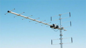
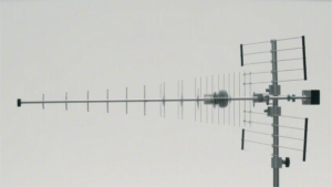
In scenarios with fixed installation directions, like industrial gateways, customized antennas can be designed in directional radiation mode, concentrating energy within a 60-degree sector in front.
This directional design not only increases communication distance in the target direction but also shields interference from other base stations to the sides and rear, increasing the average SNR by 6dB to 8dB.